Content last revised on September 26, 2026
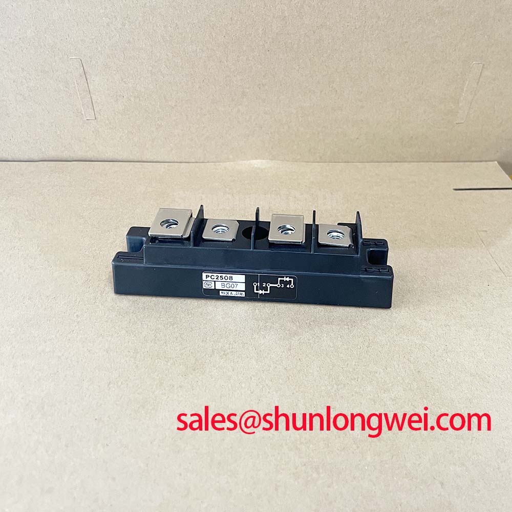
PK55GB80 SanRex 800V 55A Thyristor and Diode Module
Start commissioning by isolating the rectifier, checking the module terminals for abnormal cold-state impedance, inspecting the case and baseplate for mechanical damage, and confirming the nameplate against the required voltage and current limits. The PK55GB80 from SanRex (Sansha Electric) is a thyristor and diode module for rectifier assemblies. Potential applications, such as green hydrogen electrolyzer DC power rectifiers, require system-level engineering evaluation.
| Manufacturer | SanRex (Sansha Electric) |
| Product category | Thyristor / Diode Module |
| Repetitive peak reverse voltage, VRRM | 800 V at Tj = −40°C to +125°C |
| Repetitive peak off-state voltage, VDRM | 800 V with gate open circuit |
| Non-repetitive peak reverse voltage, VRSM | 960 V under the specified non-repetitive conditions |
| Average on-state current, IT(AV) | 55 A, single-phase half-wave, 180°, Tc = 89°C |
| R.M.S. on-state current, IT(RMS) | 86 A; operation must also satisfy the average-current and thermal limits |
| Surge on-state current, ITSM | 1000 A at 50 Hz or 1100 A at 60 Hz, half-cycle non-repetitive |
| Fusing I2t | 5000 A2s at 10 ms, 50 Hz |
| Critical on-state current rise, di/dt | 150 A/µs, gate drive IG = 100 mA, gate-current rise rate diG/dt = 1 A/µs |
| Critical off-state voltage rise, dv/dt | 500 V/µs at Tj = 125°C, linear to 67% VDRM |
| Gate trigger current and voltage, IGT / VGT | 100 mA / 3.0 V maximum at VD = 6 V and IT = 1 A |
| Thermal resistance, Rth(j-c) | 0.53°C/W; use the manufacturer's element and dissipation basis for thermal calculations |
Field Diagnostics & Commissioning: Preventing Localized Gate Hotspot Burnout in PK55GB80 Topologies
During a failed-start investigation, verify the gate circuit with the power stage isolated before applying high voltage. The maximum gate trigger specifications are IGT = 100 mA and VGT = 3.0 V under the stated test conditions; these are not maximum allowable gate-drive ratings. The firing circuit should provide a clean pulse with adequate gate current and a stable return path. Gate pulse rise time, pulse width, sustained gate current after the initial pulse peak, and the timing relationship between parallel firing channels should be checked with an oscilloscope against a known-good assembly.
A gate pulse that reaches the required trigger condition does not by itself confirm balanced current sharing. Wiring length, connector resistance, trigger-transformer behavior, and pulse timing can alter the effective gate drive at the module terminals. Multi-pulse firing schemes should therefore be validated under the actual line frequency and load conditions rather than assessed only with a low-voltage bench signal. A localized gate temperature rise may indicate an uneven trigger path, excessive electrical noise, or a mechanical connection issue; the diagnostic path should include terminal inspection and waveform comparison.
For protection coordination, the specified I2t value of 5000 A2s at 10 ms is an official device rating, not a complete fuse selection instruction. The fuse let-through characteristic, prospective fault current, clearing time, and wiring impedance must be compared by the system designer. The module’s ITSM rating of 1000 A at 50 Hz or 1100 A at 60 Hz describes a non-repetitive half-cycle surge and should not be treated as a continuous operating allowance.
When a different voltage class or current arrangement is being evaluated, engineers may also review the PK55FG120. Any substitution requires confirmation of circuit topology, gate-drive compatibility, thermal conditions, mechanical fit, and the complete manufacturer data.
Benchtop Waveform Tuning: Mitigating PK55GB80 Stress via RC Snubber Network Optimization
Use a current-limited, isolated test arrangement when examining commutation behavior. The PK55GB80 has an official dv/dt rating of 500 V/µs at Tj = 125°C, with the specified linear voltage condition reaching 67% of VDRM. This rating provides a device boundary for evaluation; it does not define the RC snubber values for a particular rectifier. Snubber resistance, capacitance, wiring inductance, source impedance, and switching frequency must be selected from measured waveforms and system fault conditions.
Observe the voltage directly at the module terminals rather than relying only on a controller-side probe point. Use appropriately rated differential or isolated measurement equipment; isolation of the test supply does not make an ordinary grounded oscilloscope probe safe at arbitrary power terminals. Ringing near the off-state voltage boundary can be associated with commutation inductance, insufficient damping, or an unsuitable measurement loop. A series saturable reactor may be considered where the system requires controlled current rise, but its magnetic behavior must be verified at the intended current and temperature. The official di/dt limit of 150 A/µs should be checked against the measured current transition in the installed topology.
Surge protection ahead of the thyristor junctions can include a coordinated MOV and snubber network, subject to the AC line voltage, energy exposure, repetition rate, and protective-device response. A TVS diode is a related transient-clamping technology, but its voltage, energy, and pulse capability must not be assumed equivalent to the requirements of a high-current rectifier. The gate circuit should be routed separately from high-current commutation paths to reduce unwanted coupling.
PK55GB80 Operational Boundaries: Ensuring Uniform Heatsink Contact Pressure
The specified Rth(j-c) value is 0.53°C/W; thermal calculations must follow the manufacturer's element and dissipation basis rather than assume this value applies to total module losses with both junctions active. Reaching the intended thermal performance depends on the complete heat-transfer path, including the baseplate, interface material, heatsink flatness, clamping method, airflow, and operating waveform. Thermal resistance should therefore be evaluated as part of the assembled rectifier rather than treated as an independent guarantee of heatsink temperature.
Before installation, clean the mating surfaces and inspect the heatsink for burrs, contamination, or distortion. Apply the approved thermal interface material as a uniform, thin layer suitable for the assembly procedure. Tighten mounting hardware progressively and evenly according to the module and heatsink mechanical documentation. Excessive localized pressure can distort the package, while insufficient or uneven pressure can increase interface thermal resistance.
⚠️ Maintenance Note: During preventive maintenance, review recorded operating-temperature and airflow trends. Remove accumulated dust from the heatsink and verify terminal tightness after the equipment has been safely isolated.
The specified average on-state current of 55 A applies to the stated single-phase half-wave condition at Tc = 89°C; the 86 A RMS rating does not override the average-current or thermal limits. Actual rectifier duty, conduction angle, ambient temperature, cooling arrangement, and both-junction operation must be assessed before applying these ratings to an electrolyzer power supply.
Field Diagnostics & Commissioning: AC Line Surge Immunity and Lightning Transients in PK55GB80 Topologies
For AC input protection, begin with the installation’s maximum line voltage, grounding arrangement, prospective short-circuit current, and surge exposure. The PK55GB80 is specified at VDRM = 800 V, VRRM = 800 V, and VRSM = 960 V. These values help establish the semiconductor voltage boundary, but they do not constitute an immunity claim for an assembled rectifier or protection system.
MOV selection should account for continuous AC stress, clamping voltage, energy absorption, repetition, thermal disconnection, and coordination with upstream fusing. RC snubber stages can reduce repetitive commutation transients when their placement and damping are confirmed through measurement. The system engineer should verify peak voltage at the module terminals during representative line surges and switching events, including the effect of cable length and enclosure bonding.
Use the Field Engineer’s Handbook as a supporting reference when building a repeatable inspection and failure-analysis workflow. The I2C bus is associated with control and monitoring devices rather than the PK55GB80 power terminals; any digital supervisory interface must be assessed separately from the thyristor firing and protection circuits.
After a surge event, compare gate trigger behavior, off-state leakage indicators, terminal condition, heatsink contact, and fuse status with a documented known-good baseline. Do not assign a single failure cause from visual inspection alone; confirm the result through controlled electrical tests within the published device ratings.