Content last revised on September 19, 2026
PM200CL1A060 Inspection and Integration Overview
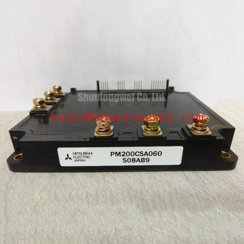
Begin the bench inspection by confirming the nameplate identity, checking the module body for visible cracking or terminal damage, and verifying that the intended replacement is rated at 600.0 V and 200.0 A. The PM200CL1A060 is a Mitsubishi Electric IPM module intended for evaluation in power conversion equipment such as a heavy duty variable frequency AC motor drive. Its published product category is Mitsubishi IPM Module; gate drive supply requirements, terminal assignments, switching characteristics, protection functions, and thermal limits must be confirmed against the applicable Mitsubishi Electric documentation before energizing a repaired assembly.
| Parameter | Specified value | Classification |
|---|---|---|
| Manufacturer | Mitsubishi Electric | Product identification |
| Part number | PM200CL1A060 | Product identification |
| Voltage rating | 600.0 V | Official supplied specification |
| Current rating | 200.0 A | Official supplied specification |
| Product category | Mitsubishi IPM Module | Official supplied classification |
These values identify the electrical class of the device, but they do not by themselves define allowable inverter bus voltage, switching frequency, overload duration, case temperature, short circuit response, or heatsink requirements. Those conditions are system determined. When integrating this IPM into a replacement drive, designers should compare the original switching topology, DC link conditions, cooling path, control interface, and protection sequence rather than selecting a replacement from voltage and current ratings alone.
PM200CL1A060 Circuit Protection & Reliability: Calibrating High Frequency Commutation Loop Inductance
During commissioning, inspect the DC link path from the capacitor bank to the IPM power terminals before applying a motor load. The positive and negative conductors should form a compact forward and return path, with the switching loop arranged to minimize enclosed area. This is a Design Consideration rather than a guaranteed characteristic of the module. Excessive stray inductance can convert rapid current change into a voltage overshoot at the switching terminals. In practical terms, the measured peak voltage is influenced by the DC link voltage, loop inductance, and current slew rate. The engineering calculation follows the relationship between the inductive term and current change, so the final clamp and insulation decisions must be based on oscilloscope measurements taken at the module terminals.
Do not treat a snubber capacitor as a universal cure. Its effectiveness depends on placement, loop impedance, capacitor technology, pulse current capability, damping, and the actual switching waveform. A remote capacitor connected through long tracks can leave the highest energy portion of the commutation loop uncontrolled. Designers should evaluate the switching node with a suitable differential probe, confirm probe connection integrity, and compare turn off overshoot at different load currents. The measured peak must be checked against the 600.0 V device rating and the system insulation coordination requirements, with an engineering margin determined by the drive designer and validated under worst case operating conditions.
Planar busbar geometry is usually preferable to widely separated conductors when the objective is to reduce loop area. Keep the high current path short, avoid unnecessary neck downs, and place the DC link decoupling element near the power switching path where the mechanical construction permits. Clearance and creepage distances remain system design requirements because the correct spacing depends on working voltage, pollution level, material group, altitude, and applicable safety standards. A single spacing value should not be presented as a universal requirement for this part.
For field troubleshooting, first isolate the DC link and follow the site discharge procedure. Inspect busbar joints, capacitor connections, laminated interfaces, and fasteners for discoloration or looseness. Then perform a controlled low energy test before returning to full power. A ringing waveform may indicate a parasitic inductance or damping issue, but it can also be affected by probe grounding, gate timing, load conditions, or control instability. Verify the signal path with a known good assembly where available. Mitsubishi Electric provides device and power semiconductor information through its Power Semiconductors and High Power Modules resource.
Preventing Spurious Faults: Negative Gate Bias vs Active Miller Clamping Guidelines for PM200CL1A060
Gate circuit evaluation should begin with the actual gate emitter waveform measured at the module terminals, not at the distant driver output. A fast voltage transition on one switching device can couple through the Miller capacitance of the complementary device and produce an unwanted gate excursion. Whether this results in false turn on depends on the driver impedance, common emitter inductance, gate loop routing, switching speed, load current, and control timing. The PM200CL1A060 supplied information establishes its voltage and current class, but it does not authorize a universal gate voltage, negative bias value, desaturation delay, or active clamp setting.
A negative gate bias is a Design Consideration that may improve turn off immunity in some driver arrangements, while an active Miller clamp can provide a low impedance path that holds the gate near its intended off state after the command transition. These functions should not be assumed interchangeable. A negative bias requires a driver and insulation architecture capable of producing and tolerating that rail, while an active clamp requires correct sensing and timing relative to the gate waveform. The system integrator should verify the original drive documentation before changing either approach.
Use short, direct gate and emitter returns, and keep the gate loop separated from high current commutation conductors. If the module provides a dedicated auxiliary emitter or control return, its use must be confirmed from the terminal drawing for the exact production variant. Do not infer pin identity from a similarly named Mitsubishi package. The control return should be referenced as the driver designer intended, while the main power return should carry the commutation current through the designated power terminals.
Desaturation protection is also system dependent. A protection circuit must distinguish a genuine overcurrent event from a transient measurement disturbance, and it must coordinate fault recognition, gate turn off, fault latching, and reset behavior. A two stage soft turn off sequence can reduce the electrical stress associated with abruptly interrupting a high current, but its timing and gate impedance require validation through controlled short circuit or fault testing performed under an approved laboratory procedure. Avoid copying a protection delay from another IPM without confirming the electrical topology and driver interface.
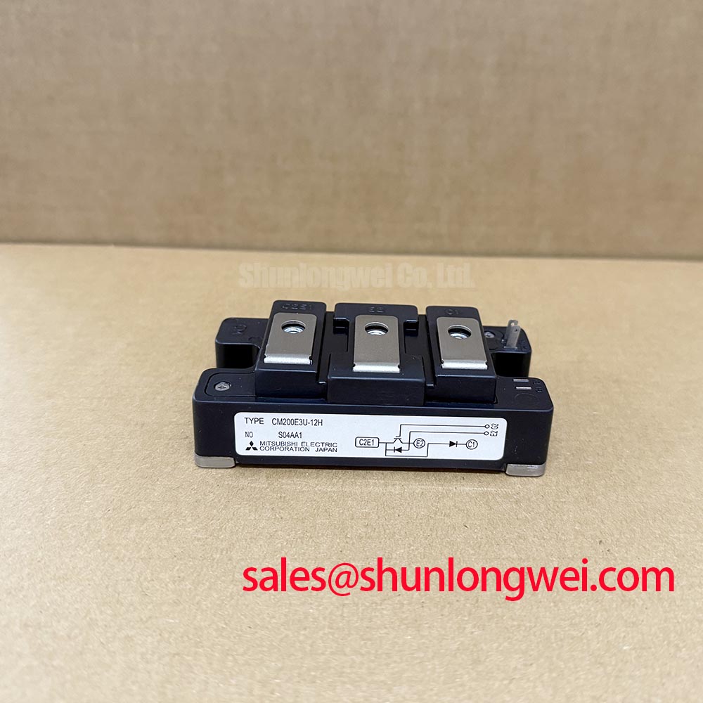
In a drive cabinet, the upstream rectifier and DC link network should be reviewed together with the inverter module. The CM100DY 12E can be examined as a neutral reference for a related front end or complementary power stage, but it should not be treated as an automatic substitute or compatibility guarantee for this IPM. Verify voltage class, current behavior, protection coordination, mechanical dimensions, and control requirements independently.
PM200CL1A060 Thermal and Electrical Optimization Guidelines
Thermal commissioning should combine electrical measurements with the actual transient thermal impedance information supplied for the applicable device revision. A heatsink that appears adequate under steady motor current can still permit excessive junction temperature during repeated acceleration, braking, or overload pulses. The relevant assessment uses the pulse duration, duty cycle, case temperature, mounting interface, cooling airflow, and the module’s transient thermal resistance curve. This is an Engineering Recommendation: the peak junction temperature must be calculated from documented thermal data and verified by measurement rather than inferred from the 200.0 A current rating.
Apply a controlled load profile and record phase current, DC link voltage, switching waveform, heatsink temperature, and fault status together. Thermal imbalance between phases may point toward unequal busbar resistance, gate timing differences, cooling contact variation, or a measurement problem. It should not be assigned to one cause without comparing all phase channels. The mounting surface should be clean and flat, and the selected interface material should be applied according to its manufacturer’s process. Mechanical pressure must remain within the applicable assembly documentation; an arbitrary torque value should not be treated as an official specification for this module.
Altitude and atmospheric radiation deserve a documented risk review when the equipment is installed at elevated locations. Neutron related single event effects and single event burnout are specialized reliability topics requiring device construction data, operating voltage history, environmental exposure assumptions, and an authoritative reliability method. No FIT rate, burnout probability, operating lifetime, or altitude derating value can be assigned to the PM200CL1A060 from its 600.0 V and 200.0 A ratings alone. Engineers should obtain relevant manufacturer guidance or an applicable reliability study before making a safety or lifetime claim.
For practical voltage margin assessment, monitor the highest switching node voltage during cold start, rated load, regeneration, line transients, and abnormal motor conditions. The system DC bus should be evaluated against the measured switching peak, not only against its nominal value. If the measured waveform approaches the device boundary, investigate busbar inductance, clamp placement, gate timing, motor cable behavior, and braking energy management. The Ultimate IGBT Knowledge Base offers a broader technical reference for reviewing switching stress, thermal behavior, and power module integration.
Control isolation is part of the thermal electrical review because common mode transients can disturb the gate command during high current switching. Optocouplers and digital isolators should be assessed using their documented common mode transient immunity, propagation delay, supply decoupling, and fault behavior. The isolation component does not independently certify the complete drive for CISPR, EN 55011, or another EMC standard. System level emissions and immunity testing remain the responsibility of the equipment designer.
Field Diagnostics & Commissioning: Differential Gate-Emitter Loop Routing in PM200CL1A060 Topologies
Commissioning measurements should use a differential probe directly across the relevant gate and emitter control terminals, with the probe loop kept physically small. Measuring gate voltage against a remote controller ground can conceal common emitter movement and produce a misleadingly clean waveform. The objective is to observe the voltage seen by the module’s control junction during turn on, turn off, fault response, and recovery. Confirm the probe’s common mode rating and isolation arrangement before connecting it to a live inverter.
Where the documented terminal arrangement includes an auxiliary emitter or Kelvin style control return, route that return separately from the high current emitter path and connect it exactly as specified. If the exact terminal drawing does not confirm such a connection, the system integrator should not assume one from package appearance. Separating the control reference from the power return can reduce mutual coupling, but the benefit depends on the complete mechanical layout, driver placement, busbar geometry, and return current paths.
Compare the high side and low side gate waveforms during the same operating condition. Look for unequal delay, excessive ringing, an unexpected plateau, or a gate excursion during the opposite device’s transition. These observations may indicate impedance mismatch, common source inductance, driver saturation, inadequate decoupling, or a control timing issue. Repeat the measurement with the motor disconnected and then with a controlled load, while preserving the same probe arrangement so that the comparison remains meaningful.
Field Alert: Isolate and discharge the DC link before inserting, removing, or reworking any control or power connector.
After the electrical checks, inspect the gate driver supply at the driver pins during switching rather than relying only on a static meter reading. Confirm that the supply remains within the driver manufacturer’s documented range and that local decoupling is positioned according to the driver layout requirements. Any reset, UVLO event, or fault latch should be correlated with the gate waveform and DC link behavior before the IPM is condemned.
For sourcing and cross checking, the CM300DXDX1 24A may be reviewed as a separate Mitsubishi Electric module option in a different electrical class. It is not a prescriptive replacement for the PM200CL1A060. Engineers should compare the official voltage and current ratings, package, terminal layout, driver requirements, thermal data, protection behavior, and mechanical fit before considering any change in a repaired heavy duty variable frequency AC motor drive.
Additional manufacturer information can be reviewed through Mitsubishi Electric Semiconductor Device Technologies. Final acceptance should be based on documented ratings, controlled switching tests, thermal measurements, protection verification, and the requirements of the complete drive assembly.