



Content last revised on October 29, 2026
SCE160DA160 Thermal Electrical Optimization: Thermal Interface Material Spreading across Practical Tuning
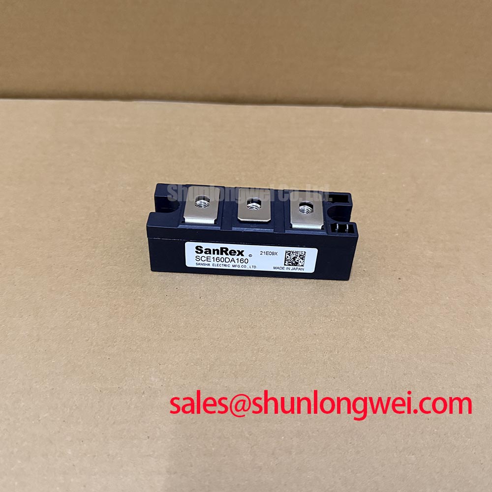
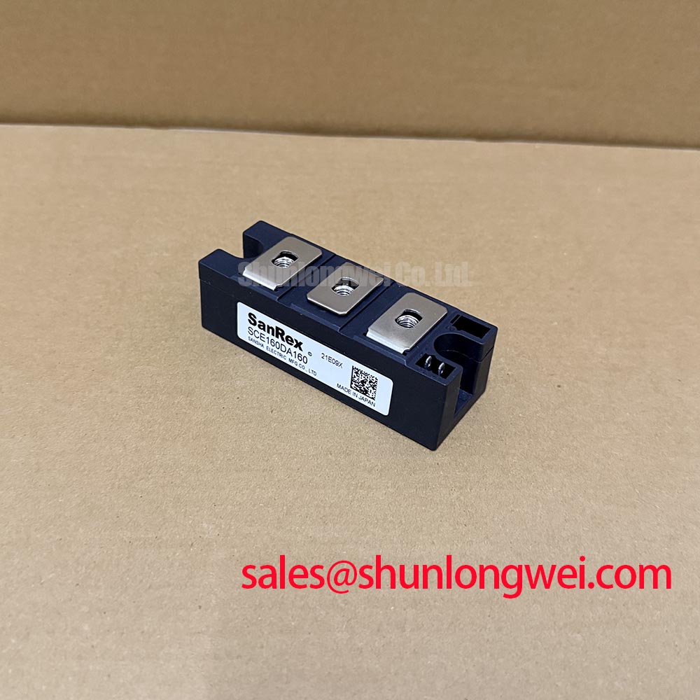
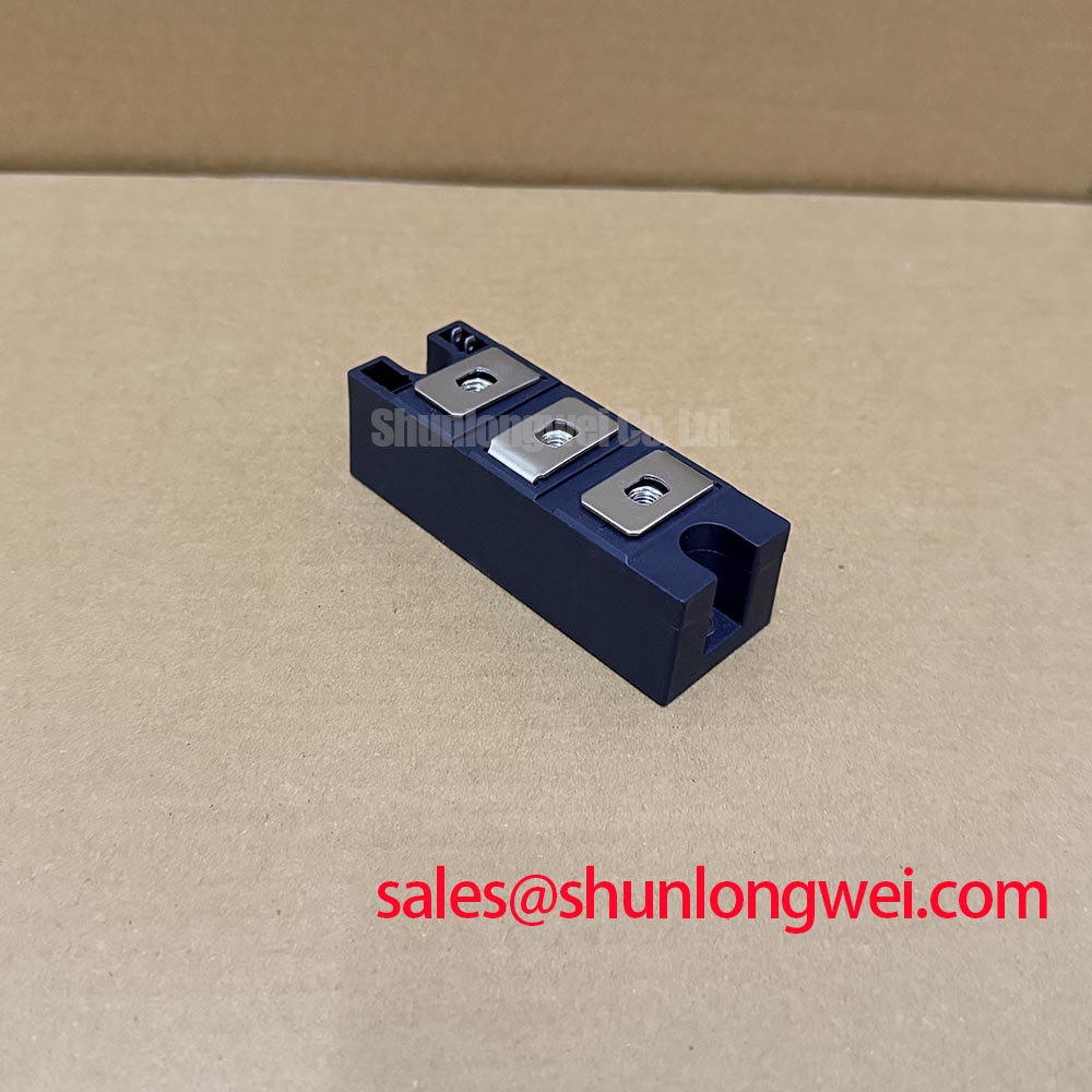
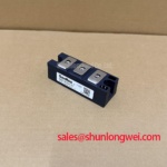
When servicing an SVC cabinet, isolate all power sources, verify absence of voltage, and discharge stored energy before checking the power terminals for abnormal cold resistance, inspecting the baseplate for distortion, and confirming that every connection is mechanically secure. The reference is the SCE160DA160 from SanRex, also known as Sansha Electric. The available product listing describes it as a Thyristor / Diode Module with a Three Phase Bridge / Dual Diode topology and a SanRex Power Module package in the Standard series. Confirm the exact internal circuit and terminal arrangement against the applicable manufacturer documentation before installation.
The supplied product information does not state a rated voltage or current value for this reference, so those limits should be taken from the applicable SanRex documentation before energizing a replacement. The manufacturer background can be reviewed through SanRex Sansha Electric power semiconductor resources. Verify the listed device identification, topology, and package description against that documentation; treat protection selection, thermal installation, and switching tests as system engineering tasks.
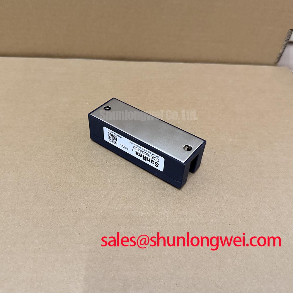
Thermal performance begins at the module baseplate and the heatsink contact surface. Remove old interface material completely, check both surfaces for burrs or localized high spots, and apply a thin, even layer of suitable thermal compound. The objective is continuous contact without forcing the module body to compensate for a warped mounting surface. Uneven pressure can increase thermal resistance and may also place mechanical stress around the power terminals.
Use the applicable SanRex mounting instructions for the permitted fastening method and torque. The available product data does not provide a model-specific torque value, so the final setting must follow the original mechanical documentation, fastener size, washer arrangement, and heatsink material. Tighten progressively in a cross pattern where the mounting layout permits it, then confirm that the baseplate remains seated after terminal wiring is installed.
Fuse coordination belongs in the same inspection record as the thermal installation. Select protective devices by comparing the system fault profile and the fuse manufacturer’s I²t data with the module’s specified withstand limits rather than by matching nominal current alone. Inspect each power terminal for correct lug seating, clean contact surfaces, and strain relief that does not pull the module sideways. Field Alert: never tighten power terminals while the cabinet is energized, and use the manufacturer’s specified mounting torque rather than a guessed value.
SCE160DA160 Thermal Electrical Optimization: Reverse Recovery Charge Temperature Coefficient Practical Tuning
During commutation, the diode section influences reverse recovery current, recovery time, switching loss, and conducted noise. For an SVC or thyristor switched capacitor bank, compare the replacement module with the original circuit topology, gate timing, line impedance, and cooling arrangement before interpreting a change in current waveform. The available listing uses the description Three Phase Bridge / Dual Diode for the SCE160DA160, but the internal circuit must be verified, and no reverse recovery figures are included in the supplied product information.
Use a properly rated differential voltage probe and current measurement method when examining the commutation interval. Look for excessive reverse recovery peak current, ringing near the device terminals, or a recovery tail that differs from the known operating condition. These observations can also be affected by wiring inductance, snubber placement, transformer leakage, and capacitor bank configuration, so the measurement point should be kept consistent between service tests.
Temperature changes semiconductor recovery behavior and can shift the balance between conduction loss and switching loss. Record heatsink temperature, line condition, firing angle, and capacitor status alongside the waveform. This creates a useful service comparison without assigning an unverified temperature coefficient to the module. The system designer should determine acceptable recovery stress from the actual thyristor and diode ratings, the fuse coordination data, and measured transient margins.
For a separate device evaluation within the same service workflow, engineers may review KD324510 as another product reference. Compatibility is not established; mechanical dimensions, topology, terminal arrangement, electrical ratings, drive requirements, and thermal requirements must be compared before procurement or installation.
Transient Dynamics and Electrical Design: Coordination of Primary Spark Gaps and MOVs on SCE160DA160
AC input protection should be coordinated from the incoming surge path toward the module terminals. A primary spark gap, where used by the system architecture, provides upstream surge diversion, while MOVs and RC snubber stages help limit voltage stress reaching the semiconductor junctions. The protection network must be evaluated against the installation category, prospective surge current, line voltage, and any applicable IEC 61000-4-5 surge immunity test requirements.
Choose MOV working voltage and energy capability from the actual AC network and surge environment. Do not select a clamp level solely from the module name or topology. Place suppression components with short, controlled connections so that wiring inductance does not create a second voltage peak at the semiconductor terminals. The RC snubber should be assessed for damping, leakage current, pulse energy, and interaction with the capacitor bank and line reactor.
Fuse selection remains part of the transient strategy. The fuse must interrupt abnormal current while remaining coordinated with the module’s permitted surge and fault conditions as documented by SanRex. Where the SVC includes a separate rectifier or front end, the surrounding topology can be reviewed with the CVM75BB160 reference, while keeping its ratings and application separate from the SCE160DA160 evaluation.
Before returning the cabinet to service, verify terminal polarity and phase order and inspect snubber and MOV connections. During controlled commissioning, compare the measured transient waveform with the system’s established voltage margin. The Field Engineer’s Handbook provides a practical reference for structured testing and failure analysis. Additional semiconductor application context is available from Shindengen power semiconductor resources.