

Content last revised on September 20, 2026
SK50DA100D Circuit Protection & Reliability: Verifying Module Terminals
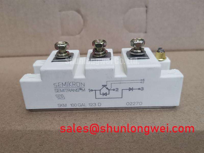
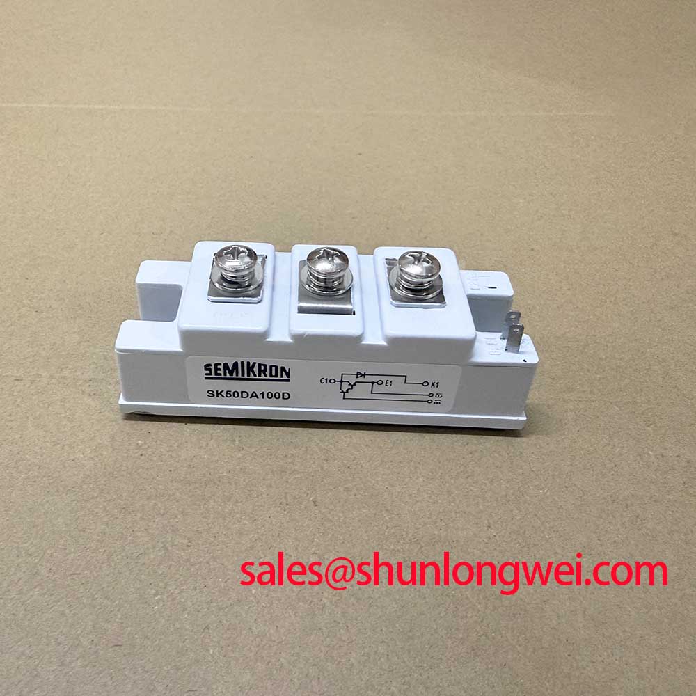
With all power isolated and the DC link verified discharged, inspect the SK50DA100D housing, terminals, mounting face, and connected conductors before any resistance test. The available official identification data lists a 50.0A current rating, a Semitrans housing, and a standard industrial working-voltage classification; the original equipment documentation must be consulted for the complete electrical limits, terminal assignment, and approved connection scheme.
| Manufacturer | Semikron |
|---|---|
| Product model | SK50DA100D |
| Current rating | 50.0A Official Specification |
| Housing | Semitrans Official Specification |
| Working-voltage classification | Standard Industrial Rating; verify the applicable voltage specification in the original documentation |
Begin by matching every power connection against the equipment schematic, because the SK50DA100D is a diode module and does not establish a Kelvin emitter or gate terminal. A Kelvin emitter return should never be assumed from the Semitrans outline or from a similarly shaped module. Where the original circuit documentation explicitly provides a separate auxiliary emitter reference for another controlled semiconductor stage, that driver return should follow the documented low-current path instead of sharing the main load-current emitter route.
This is a Design Consideration: separating a sensitive driver reference from the high-current switching return reduces common inductance coupling in a controlled semiconductor stage. Shared return impedance can alter the gate reference seen by a driver during current transitions, which may appear as irregular switching waveforms, unexplained gate ringing, or inconsistent protection events. These symptoms do not by themselves indicate that the diode module has failed. Measure the installed circuit against a known-good channel with properly rated differential probing before changing the gate-drive arrangement.
For a heavy-duty variable frequency AC motor drive, review the complete power and control return paths from the driver board to the module and back to the DC-link capacitor bank. Inspect for loose terminal hardware, heat-discolored conductors, cracked solder joints on the driver board, and harness routing that places a control return alongside a high-current conductor. The original board layout, not a generic layout rule, determines whether a dedicated auxiliary return is present and how it must be connected.
When evaluating related drive hardware, SKM100GB063D can be reviewed as a separate module reference, but its terminal configuration, current capability, voltage rating, thermal interface, gate-drive requirements, and mechanical fit must be independently verified. Similar product families do not establish drop-in compatibility.
Field Alert: Disconnect and verify discharge of the DC bus before moving module cables, because retained energy and an incorrect reconnection can damage the power stage or test equipment.
SK50DA100D Circuit Protection & Reliability: Calibrating Regenerative DC Bus Voltage Surge Dissipation
A decelerating motor can return energy to the DC bus, so the first repair question is whether the original drive uses a braking path, a regenerative supply path, or another documented method of handling returned energy. The SK50DA100D official data provided here identifies a 50.0A rating and Semitrans housing, but it does not specify an internal braking IGBT, braking resistor, or regenerative-control function. Those functions must be identified from the host drive schematic and the original service documentation.
As a Design Consideration, assess the braking resistor, braking switch, bus-voltage sensing circuit, precharge path, and associated wiring as one energy-management chain. A rise in DC-bus voltage during rapid deceleration may be associated with the commanded ramp, load inertia, braking-path availability, sensing accuracy, or a connection issue. It should be evaluated with suitable measurement equipment and against the machine's documented operating limits rather than attributed to one component from a single symptom.
Gate-drive interlock and dead-time behavior belong to the drive-control system and are not functions of the SK50DA100D diode module itself. Complementary switching commands in an associated controlled semiconductor stage require a controlled non-overlap interval so that the intended switching devices cannot conduct simultaneously during a transition. The appropriate timing is system-determined and should be confirmed with the installed driver, power topology, switching conditions, and waveform measurements. Do not transfer timing values from an unrelated module or controller board.
In a drive cabinet where other power stages are being reviewed, SKM75GB07E3 may be considered as a separately specified device in the wider converter assembly. Its presence in a comparison does not establish that it is a substitute, a braking device, or an electrically interchangeable part for the SK50DA100D.
Field Diagnostics & Commissioning: Evaluating Thermal Capacitance vs Heat Sink in SK50DA100D Topologies
Before recommissioning, remove contamination from the heatsink interface, inspect the module base contact area for damage, and verify that the mounting pattern and hardware match the original assembly. The Semitrans housing identifies the mechanical family, not the exact tightening requirement. Follow the equipment documentation and the applicable Semikron documentation for the specific mounting arrangement, fastener hardware, insulation parts, and thermal-interface material.
Thermal capacitance and transient thermal impedance are Design Considerations when a drive experiences pulsed loading. A heatsink can remain relatively cool while semiconductor junction temperature rises during short high-loss events, because heat requires time to move through the module and interface into the heatsink. Engineers commonly model this behavior using transient thermal impedance networks, then compare calculated junction conditions with the device limits stated in the applicable manufacturer documentation. No junction-to-case thermal value or transient thermal curve is established by the supplied SK50DA100D identification data, so a numerical junction-temperature calculation should not be made without the correct datasheet.
During fault investigation, inspect airflow direction, blocked fins, fan operation, enclosure filters, heatsink flatness, mounting pressure consistency, and signs of repeated thermal cycling at terminals or PCB connections. A repeated overtemperature indication can also arise from temperature-sensor wiring, control thresholds, switching behavior, loading conditions, or cooling degradation. Capture operating current, heatsink temperature, bus voltage, and relevant drive alarms together so that the power-stage result is evaluated in context.
For broader background on the relationship between thermal interfaces, package construction, and cooling strategies, see The Advanced Thermal Management Revolution. This material supports system-level investigation and does not replace the model-specific thermal documentation required for a final assessment.
Semikron-Danfoss maintains product-family information through its Power Electronics and Modules Official Hub. Use the manufacturer source and the original drive documentation to establish the exact thermal characteristics and permissible operating boundaries for the installed unit.
Transient Dynamics & Electrical Design: DC Link Capacitance Bank Layout and Low ESL on SK50DA100D
Inspect DC-link capacitor connections, laminated conductors or busbars, module terminal hardware, snubber components, and gate-drive routing before treating a switching transient as a module-only issue. During a current transition, peak voltage is influenced by the DC-link voltage plus the voltage developed across stray inductance as current changes. This Engineering Calculation principle explains why physical loop geometry, conductor length, connection symmetry, and capacitor placement affect measured overshoot.
The layout objective is to minimize parasitic loop inductance where fast switching currents circulate, so commutation-related inductive overshoot is suppressed. The final geometry, capacitor selection, snubber implementation, and allowable peak margin are determined by the complete converter system. Verify them through controlled switching tests using suitable high-voltage, high-bandwidth measurement practice, while comparing peak results with documented system and device limits.
Electrolytic capacitor condition, film-capacitor connection integrity, and busbar contact resistance should be checked during a repair assessment. Swollen capacitors, loose fasteners, deteriorated insulation hardware, and asymmetrical conductor routing can alter the behavior of a power stage. A waveform that differs from a known-good phase may indicate a layout, driver, measurement, or component-path issue; use the equipment schematic and comparable measurements to isolate the condition.
The Semikron MiniSKiiP Power Modules resource describes a different module product line and is useful only as a manufacturer context reference. It must not be used to infer SK50DA100D electrical characteristics, package dimensions, terminal functions, or system compatibility.