




Content last revised on October 23, 2026
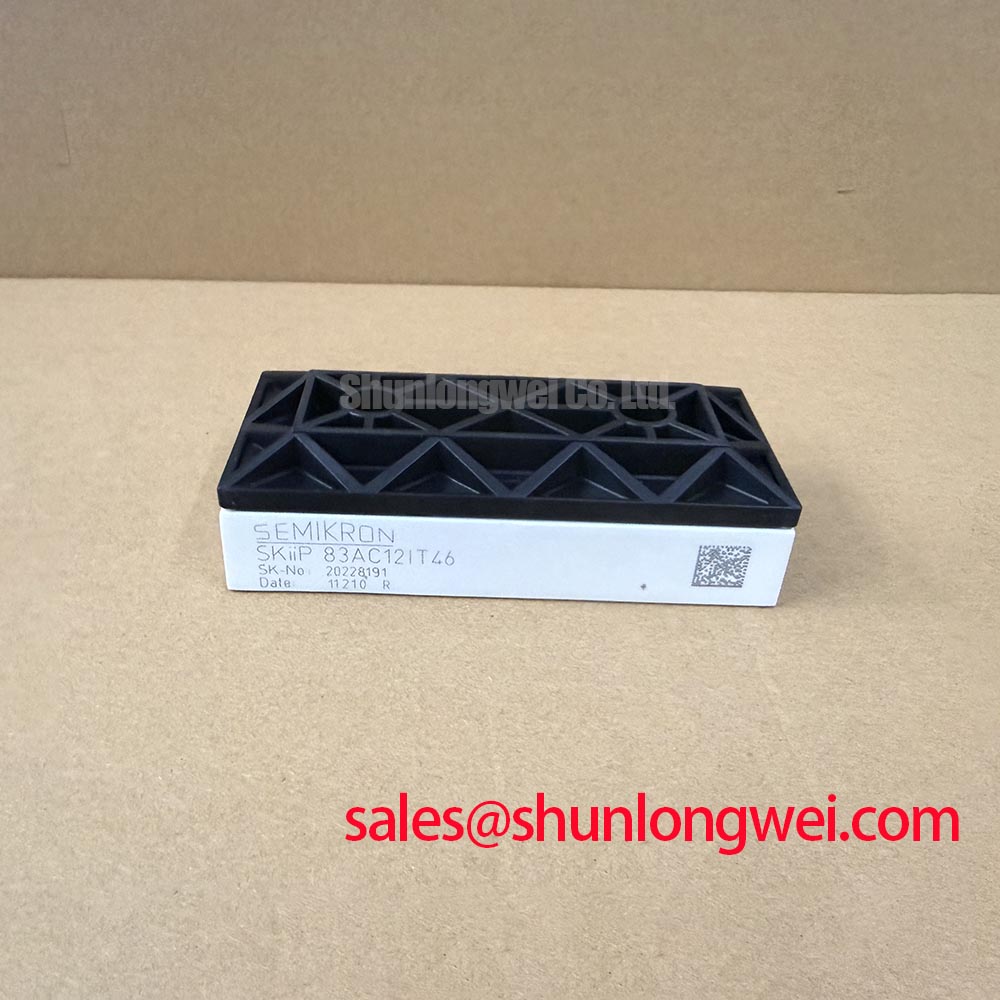
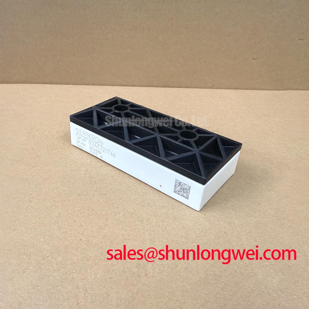
SKIIP 83AC121T46 Identification and Pre-Test Checks
- Isolate the DC link, verify discharge, and disconnect the gate driver before checking power-terminal resistance on the SKIIP 83AC121T46.
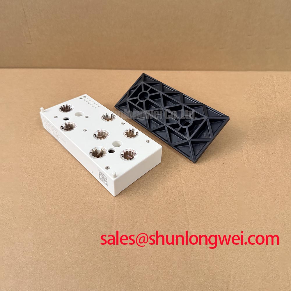
- Record terminal markings and compare the mounting interface, contact positions, and driver connections with the equipment drawings.
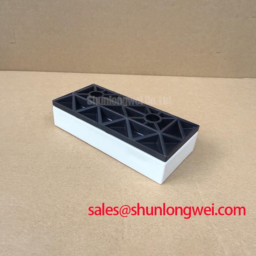
- Inspect the heatsink contact surface, mounting hardware, and accessible insulation surfaces for contamination, damage, or uneven seating.
- Check oscilloscope probe ratings and connection points before capturing gate-emitter voltage or collector-emitter switching waveforms.
The Semikron SKIIP 83AC121T46 is an IGBT power module with a specified voltage rating of 1200 V. Confirm its current ratings, rating conditions, and exact package configuration in the model-specific datasheet. These identifiers provide the starting point for electrical and mechanical compatibility assessment; commissioning also depends on the actual circuit connections, cooling arrangement, and protection implementation.
| Product identification | Specification | Parameter status |
|---|---|---|
| Model | SKIIP 83AC121T46 | Product identifier |
| Manufacturer | Semikron | Manufacturer identification |
| Voltage rating | 1200 V | Official Specification |
| Current rating | Consult model-specific datasheet | Operating conditions govern usable current; do not infer the rating from the part number |
| Package configuration | Consult model-specific datasheet | Verify the exact mechanical interface and terminal arrangement |
| Detailed integration limits | Consult Datasheet | Terminal arrangement, rating conditions, gate limits, mounting requirements, insulation test conditions, and short-circuit capability |
As a Design Consideration, engineers evaluating this device for a heavy-duty variable-frequency AC motor drive should compare the existing power-stage schematic and cooling interface before treating a matching nameplate rating as replacement approval. The technical discussion below separates the stated product ratings from system-dependent inspection and gate-drive practices.
Before Waveform Tuning: Insulation Assessment and Suspected Substrate Damage on SKIIP 83AC121T46
Separate the module from connected driver electronics and suppression networks before performing an insulation assessment under the applicable service procedure. An installed assembly can contain parallel leakage paths, capacitors, and sensitive circuitry that change the measurement or make a high-voltage test inappropriate. Identify the insulation barrier from the electrical and mechanical drawings rather than assuming that every mounting surface is an accessible conductive baseplate.
Design Consideration: an insulation-resistance reading evaluates electrical leakage under the selected test conditions; it does not directly identify a ceramic microcrack. Surface contamination, moisture, fixture leakage, and connected equipment can influence the result. A suspected internal defect therefore requires an approved diagnostic route, not a visual or resistance-only declaration about the internal substrate.
Neither a specific insulation-test voltage nor an acceptance resistance should be assigned to this model from a generic workshop checklist. Use the manufacturer-approved test arrangement and the equipment service acceptance criteria, including the terminal grouping, test duration, and discharge procedure. Record the instrument, environmental conditions, and connection arrangement so that repeated measurements remain comparable. A withstand test and an insulation-resistance test are different procedures and should not be substituted for one another.
Accessible contamination deserves attention before waveform tuning. Inspect insulating surfaces and the surrounding board for conductive deposits, tracking marks, displaced hardware, or residue bridging intended spacing. Follow the equipment-approved cleaning method and allow the assembly to dry before retesting. Creepage and clearance assessment belongs to the complete installed arrangement, including adjacent conductors and the expected pollution environment; the module voltage rating alone does not establish the necessary spacing.
The manufacturer’s Semikron-Danfoss SKiiP® Technology information provides package-technology context, while the Semikron MiniSKiiP® Power Modules page supports product-family orientation. Family-level information should remain separate from conclusions about the internal construction or test limits of a particular ordering code.
Engineering Recommendation: inspect the thermal contact arrangement while the assembly is accessible. Check mating-surface condition, heatsink flatness against the applicable drawing, and evidence of uneven mechanical loading. Apply the specified thermal interface material and fastening procedure rather than adopting generic grease thicknesses or bolt torques. The correct assembly method depends on the package interface and mounting system.
A temperature imbalance can justify checking contact pressure, interface coverage, cooling flow, and electrical loading together; it does not independently prove substrate damage. The Advanced Thermal Management Revolution provides broader thermal-management background for interpreting these interfaces without establishing this model’s internal materials. After reassembly, compare temperature measurements at consistent locations and loading conditions rather than judging the installation from an isolated surface reading.
SKIIP 83AC121T46 Operational Boundaries: Evaluating Fault-Clearing Dynamics and Type-I/II Short Circuits
Trace the complete fault-clearing path from collector-emitter sensing to gate discharge before applying power. The relevant sequence includes sensing, blanking, filtering, isolation propagation, driver response, and the controlled current fall. A fast comparator alone does not establish that the complete assembly clears a fault within the semiconductor’s permissible short-circuit interval.
Design Consideration: a type-I short circuit describes turn-on into an existing fault, whereas a type-II event develops while the device is already conducting. These conditions impose different stresses on sensing and turn-off behavior. The product’s voltage and current ratings do not establish a short-circuit withstand time, so a generic microsecond target must not be presented as the SKIIP 83AC121T46 short-circuit safe operating area.
Desaturation protection evaluates collector-emitter behavior during commanded conduction, with an appropriate blanking interval to avoid interpreting the normal switching transition as a fault. Excessive blanking can delay protection, while insufficient blanking can create nuisance trips. Engineering Recommendation: evaluate the sensing waveform and protection timing together with the gate waveform, using the actual driver circuit and the manufacturer-defined operating boundaries.
Controlled fault turn-off can reduce the rate at which fault current collapses and thereby limit inductive overvoltage. A two-stage soft-turn-off arrangement is one possible driver strategy, not an established feature of this module. Its intermediate gate behavior, discharge path, and final off-state control require coordination with the semiconductor limits and the power-loop inductance. Slowing turn-off indiscriminately can also increase energy dissipation during the fault.
Gate-driver sourcing and sinking capability should be assessed from the gate-charge behavior, desired switching transition, driver output impedance, and permitted dissipation. External gate resistance works with these elements rather than acting as an independent speed setting. Check the driver’s pulse capability and supply stability during transitions; a driver that reaches its own current limit can produce different gate waveforms from those expected from the resistor value alone.
Dead time requires the same system-level treatment. Evaluate actual turn-off delay, current decay, propagation mismatch, and the complementary device’s turn-on behavior across operating conditions. Increasing dead time without measurement can alter conduction losses and waveform quality, while insufficient separation can permit cross-conduction. Thyristor trigger-current and trigger-voltage criteria are not substitutes for IGBT gate-drive analysis.
In the surrounding power topology, trace the incoming supply stage, DC-link charging path, auxiliary supplies, and fault-inhibit connections separately. If PS11032 appears in the same sourcing review, establish its documented circuit function before assigning it a front-end or auxiliary-stage role. A linked product name does not demonstrate electrical compatibility or coordinated fault protection with this module.
Protection validation should proceed through the equipment’s approved, energy-limited test procedure. Confirm fault latching, restart inhibition, and control-supply behavior before considering higher-energy testing. Retain synchronized traces of the fault indication, gate voltage, and power-terminal voltage so that protection delay can be distinguished from the subsequent turn-off transient.
Preventing Spurious Faults: Balancing Switching Dissipation vs di/dt Guidelines for SKIIP 83AC121T46
Capture gate-emitter and collector-emitter waveforms with suitable differential probing before changing external turn-on or turn-off resistance. Excessive probe-loop area, an unsuitable reference point, or inadequate common-mode performance can create apparent ringing that does not represent the voltage at the module terminals. Keep the measurement arrangement consistent when comparing adjustments.
Design Consideration: increasing turn-on resistance generally slows the switching transition and can reduce current slew rate, but it can also increase switching energy. Turn-off resistance influences gate discharge, voltage overshoot, and susceptibility to unwanted gate movement. Separate resistance paths offer tuning flexibility only where the existing driver topology supports them; they are not permission to modify a service assembly without circuit review.
Miller coupling is particularly relevant when the complementary switch changes voltage rapidly. Current coupled into the gate circuit can raise the off-state gate voltage, especially where the discharge path has excessive impedance or shared inductance. Evaluate the gate return routing, driver placement, and available sink capability before treating a larger resistor as the universal cure. Any clamp or off-state bias strategy belongs to the verified driver design.
Pro Tip: Keep outgoing and return commutation paths closely coupled and geometrically balanced where practical, then use controlled double-pulse measurements to verify overshoot and switching-loss trade-offs within the approved test envelope.
When assessing the 1200 V boundary, examine the measured peak collector-emitter voltage at the relevant operating conditions, including switching transients. For current capability, relate the intended current waveform to cooling performance, conduction losses, switching frequency, and the applicable datasheet rating conditions. Engineering Recommendation: establish derating through the equipment’s thermal and electrical validation rather than assigning a universal margin percentage.
Replacement comparison should also distinguish semiconductor ratings from functional architecture. The PM15RHB120 can be included in a broader power-module comparison, but it is not established here as an interchangeable replacement. Compare circuit configuration, driver requirements, protection interfaces, terminal mapping, mounting arrangement, and thermal characteristics before considering any substitution. An IPM category label alone does not establish which control or protection functions are present.
For a nuisance-trip investigation, correlate the fault timestamp with the gate waveform, DC-link disturbance, and load condition. A trip synchronized with a switching edge can justify inspecting common-mode coupling, sensing layout, and blanking behavior; it does not uniquely identify a defective module. Check auxiliary supply stability and signal return routing alongside the power waveform, especially after a driver-board repair.
Change one tuning variable at a time and document the resulting transition shape, peak voltage, protection behavior, and thermal response. After an acceptable waveform is obtained, repeat the relevant checks across the intended operating envelope and restore the production measurement configuration. Retain the approved resistor configuration and captured traces with the equipment service record so that subsequent maintenance can distinguish an intentional adjustment from an undocumented change.