
Content last revised on September 18, 2026
Assembly Integrity & Layout Architecture: Implementing Optocoupler vs Digital Coreless Transformer for PM15RHB120
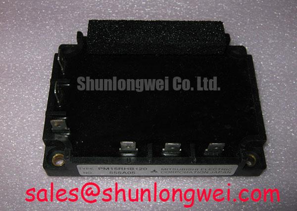
When assessing a PM15RHB120 installation in light industrial automation or a multi joint robotic articulator drive, begin at the physical interface between the control board and the power section. The 1200.0 V and 15.0 A ratings define the module’s published electrical boundary, but they do not establish the isolation capability of an external gate drive board. Isolation barriers, creepage paths, clearances, connector spacing, and control ground routing are properties of the complete drive assembly and must be checked at board level.
Optocoupler isolated drivers and digital coreless transformer isolated drivers can both be considered where an inverter controller needs galvanic separation from a power stage. This is a Design Consideration, not a PM15RHB120 factory feature claim. The choice should follow the original drive architecture, the isolation requirements of the end equipment, the expected common mode switching environment, and the qualification data of the selected driver component. If a replacement control board specifies reinforced isolation or a stated common mode transient immunity requirement, those requirements should be verified from that board’s documentation rather than transferred to the power module.
Keep the isolated driver return path controlled and physically close to its associated gate command path. This layout principle helps reduce parasitic coupling that can disturb switching commands when the power node changes rapidly. Wide separation between the noisy power loop and low level control traces, carefully assigned return paths, and direct observation of gate to emitter behavior during commissioning are practical checks. A ringing waveform, unexplained control resets, or irregular switching transitions may indicate coupling through layout, grounding, supply decoupling, or a damaged driver path. These conditions should be investigated with suitable isolated measurement methods against a known good signal path.
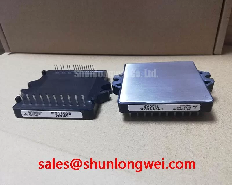
For repair work, it is useful to compare the installed PM15RHB120 board against the removed board at the connector level. Verify that every control connection reaches the intended driver channel and that no harness strain transfers mechanical force to small signal terminals. The Mitsubishi Electric Power Semiconductors and High Power Modules resource provides manufacturer level context for power semiconductor product families, while the original equipment schematic remains the controlling reference for a particular machine.
A CM100DY 12E can be reviewed as a separate 1200 V class power semiconductor reference during a documented engineering comparison, but package construction, current rating, pin arrangement, drive method, thermal interface, and protection implementation must all be validated independently. A shared voltage class alone does not establish replacement compatibility.
Assembly Integrity & Layout Architecture: Implementing Fault Clearing Dynamics: Type I/II Desatur for PM15RHB120
Fault clearing begins with observing what the existing machine monitors, where it monitors it, and how it commands shutdown. The PM15RHB120 has a published rating of 1200.0 V and 15.0 A, but no short circuit withstand time, desaturation threshold, internal protection sequence, or soft turn off behavior is established here as an official specification. These values must not be assumed from the voltage rating or from another Mitsubishi module family.
Type I and Type II desaturation methods are Design Considerations for external driver and protection circuits. A desaturation circuit generally observes the voltage behavior of a conducting power switch to identify a potential overcurrent condition. Its practical validity depends on blanking behavior, sensing path integrity, switching noise, the driver’s response characteristics, and the safe operating information available for the exact module. Engineers should verify that the detection path is coordinated with the original module documentation and with measured switching behavior under controlled test conditions.
Where a controller uses staged shutdown, the purpose is to reduce the chance that an abrupt interruption of fault current creates an excessive inductive voltage transient. The final response is determined by the complete system: DC link arrangement, busbar geometry, cable length, snubber network, drive settings, motor load, and protective hardware all influence the result. An Engineering Recommendation is to inspect the shutdown waveform with properly rated instrumentation and verify peak voltage margins against the DC link voltage during switching tests. Do not treat a generic desaturation arrangement as evidence that a particular PM15RHB120 installation has adequate fault protection.
High speed semiconductor fuses can be part of a fault isolation strategy, yet fuse coordination requires the actual fuse time current data, the upstream source capability, the equipment protection logic, and the documented surge capability of the protected power stage. Fuse clearing energy cannot be selected safely from the module’s 15.0 A rated current alone. If a fuse has operated, examine the DC link capacitors, bridge wiring, motor cable, gate driver outputs, and load insulation before fitting a replacement module. A repeated fuse operation can arise from several different system faults and should not be assigned to one cause without measurement.
In systems that include an upstream rectifier or power interface, the relationship between source protection and inverter shutdown should be reviewed as one coordinated event. The SKIIP37AC12T4V1 is an example of a related power device that may appear in broader power conversion assessments, although its electrical and mechanical requirements must be reviewed independently from the PM15RHB120.
Assembly Integrity & Layout Architecture: Implementing Sizing Braking Resistors and Chopper Trans for PM15RHB120
During motor deceleration, a rotating load can return energy to the DC link. In a robotic articulator or automation axis, the quantity of returned energy depends on moving mass, speed, commanded deceleration, gravity effects, duty cycle, and the behavior of other axes. A braking chopper and braking resistor are therefore system components whose selection cannot be derived from the PM15RHB120 voltage and current ratings alone.
The first maintenance check is architectural. Determine whether the original equipment directs regenerative energy into a dedicated braking chopper, a common shared DC bus, an active front end, or another defined energy handling path. Inspect the resistor enclosure, connection integrity, thermal protection contacts, and chopper control wiring. A resistor with visible heat distress, an open thermal switch, loose termination, or compromised enclosure ventilation can affect DC link behavior, but further electrical measurement is necessary before identifying the failing assembly.
Braking resistor sizing is an Engineering Calculation based on the machine’s permitted DC link range, the energy of each deceleration event, the frequency of those events, and the resistor’s pulse and continuous thermal capability. The system engineer should calculate and validate these conditions using the original drive data and the actual motion profile. It is not appropriate to prescribe a resistance value, chopper current setting, or energy margin for the PM15RHB120 without those inputs.
Layout remains important because the chopper loop can carry pulsed current. Minimize loop inductance to suppress turn off inductive overshoot, keep power conductors mechanically secure, and verify peak voltage behavior during controlled switching tests. Cable routing should also prevent braking resistor wiring from coupling noise into command or feedback wiring. These are Design Considerations for the complete equipment, not published internal construction details of the module.
When several inverter legs operate from a shared supply, simultaneous deceleration events can alter the energy distribution seen by the braking path. Designers should verify the operating sequence across axes rather than evaluating a single motor channel in isolation. This is particularly relevant where a multi joint robotic arm can accelerate one section while another section decelerates.
Transient Dynamics & Electrical Design: Active Miller Clamp Implementation on PM15RHB120
Gate loop stability should be checked at the module terminals with reference to the original drive schematic. During switching, voltage movement at a power terminal can couple through device capacitances into a gate circuit. If the off state gate path has excessive impedance, this coupling can contribute to unintended gate voltage movement and possible cross conduction. The magnitude depends on the complete layout, driver output behavior, gate resistor network, DC link loop, probe method, and switching conditions. No gate charge, Miller capacitance, or recommended gate bias value is stated here as an official PM15RHB120 parameter.
An active Miller clamp is a Design Consideration for a compatible external gate driver. It is intended to provide a low impedance gate to emitter holding path after the switch is commanded off, reducing susceptibility to induced turn on during high transient conditions. Whether it is appropriate depends on the existing driver design and the module documentation. The system integrator should verify the driver’s clamp activation behavior, output current capability, isolation arrangement, and interaction with the controller’s dead time before modifying an established drive board.
Negative gate bias is also a driver level design choice, not a value that should be imposed from this product page. The required off state bias, if any, must be confirmed from the original PM15RHB120 support documentation and from the driver component limits. A negative bias network that is unsuitable for the gate driver or module can create its own reliability and measurement problems. Engineers should check for gate overshoot, ringing, timing mismatch between complementary commands, and common mode ground movement using correctly referenced instrumentation.
Dead time exists to prevent both devices in a switching leg from conducting at the same time, but its final value is system determined. It must accommodate the real switching transition, propagation delays, temperature behavior, driver asymmetry, and control timing of the installed equipment. A command trace that appears correct at the controller output may still differ at the power stage because of isolation channel delays or gate loop disturbances. Compare gate signals at the relevant terminals and evaluate them alongside the switching node waveform.
For wider context on inverter efficiency and switching behavior, see Unlocking Efficiency in Industrial Drives. It should be used as technical background rather than as a substitute for the PM15RHB120 documentation. Mitsubishi Electric also publishes technology context through its Global Semiconductor Device Technologies pages. For a repaired industrial drive, the decisive checks remain correct terminal mapping, verified insulation and control paths, measured switching behavior, and operation within the official 1200.0 V and 15.0 A ratings.