

Content last revised on September 15, 2026
PM50RSE120 Ratings and Replacement Checks
Before energizing a replacement, isolate the DC bus, inspect the package and terminals, and verify the nameplate boundary of PM50RSE120 against the inverter service documentation. A cold electrical comparison with a known serviceable unit can help identify an open connection or an unexpected low impedance, but it is not a substitute for controlled semiconductor testing.
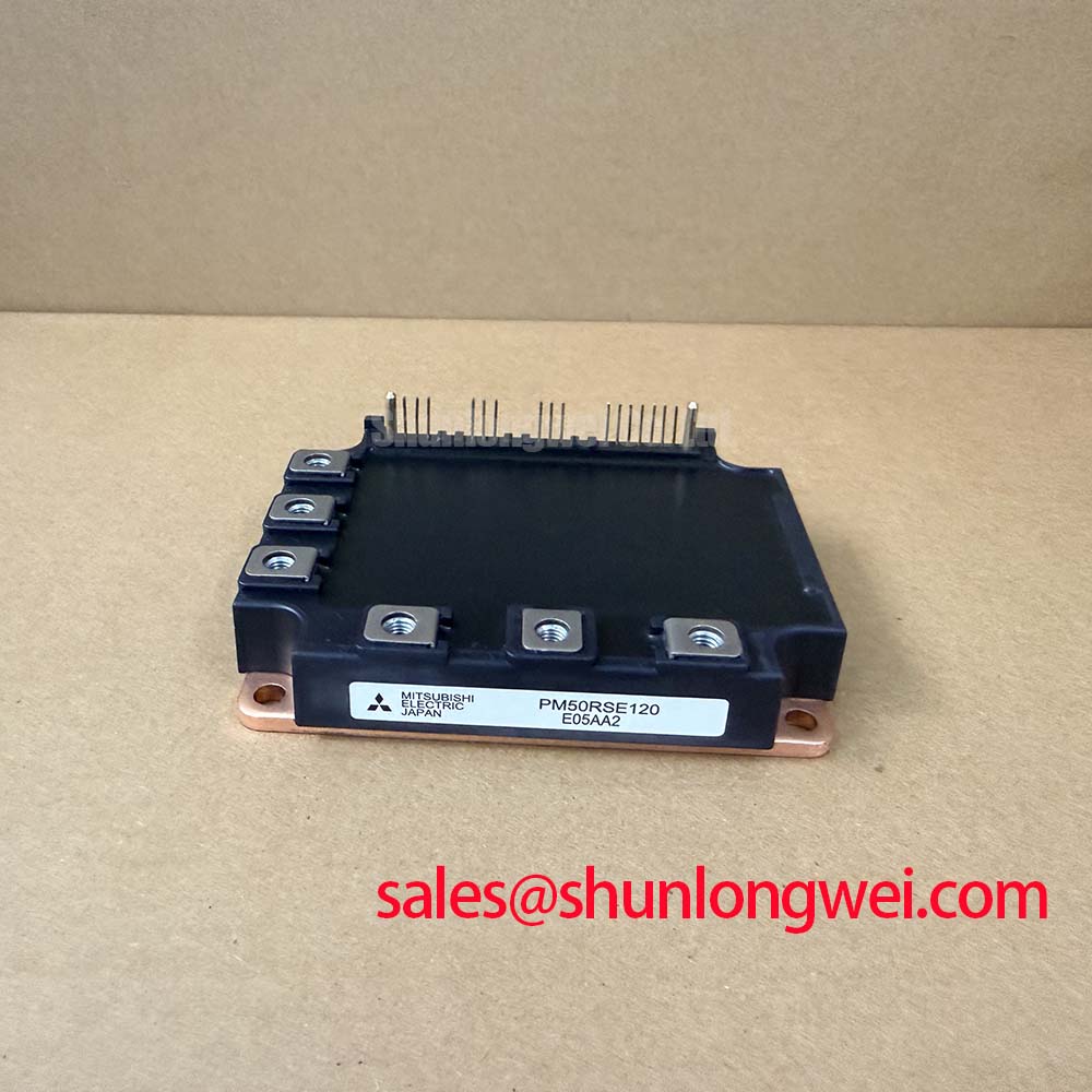
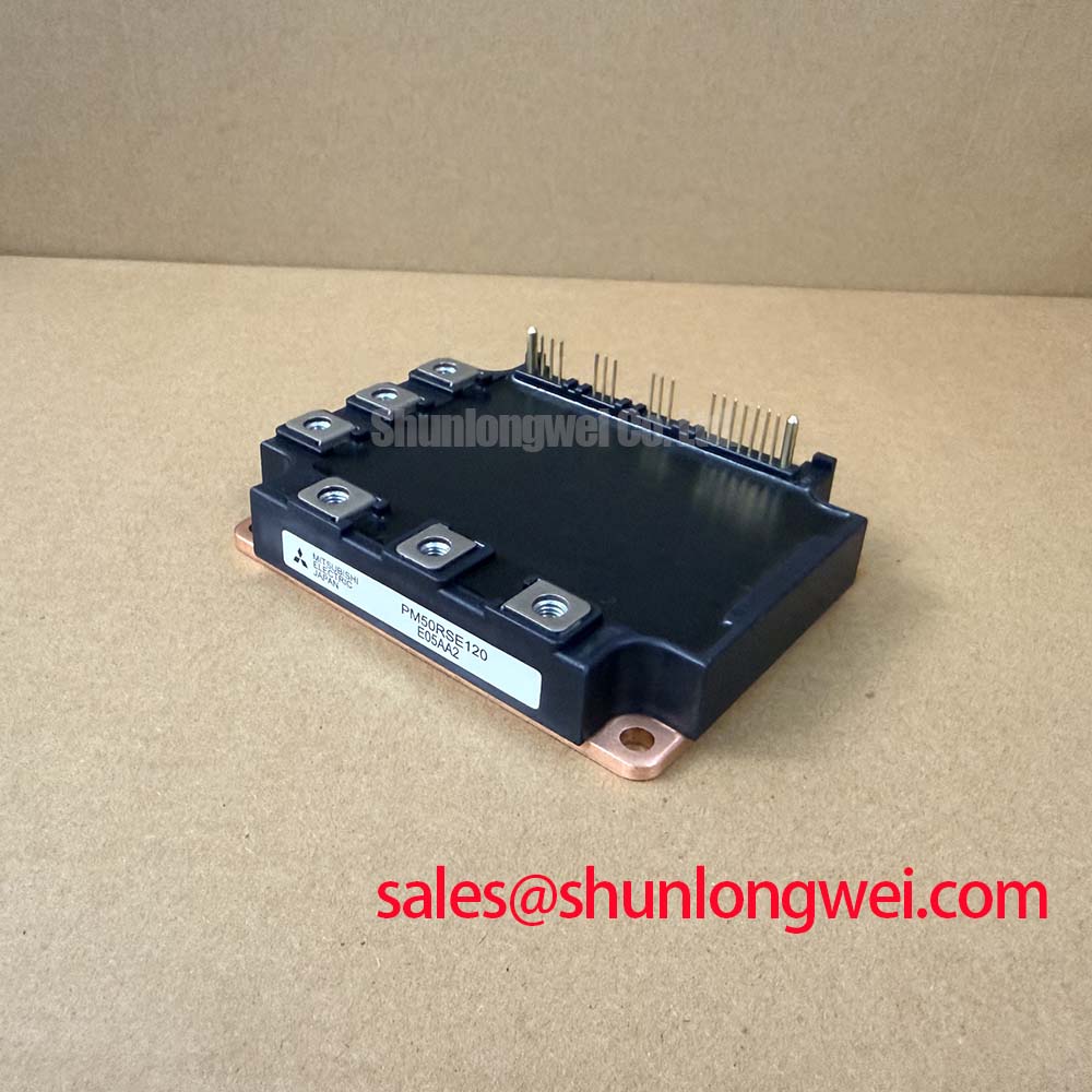
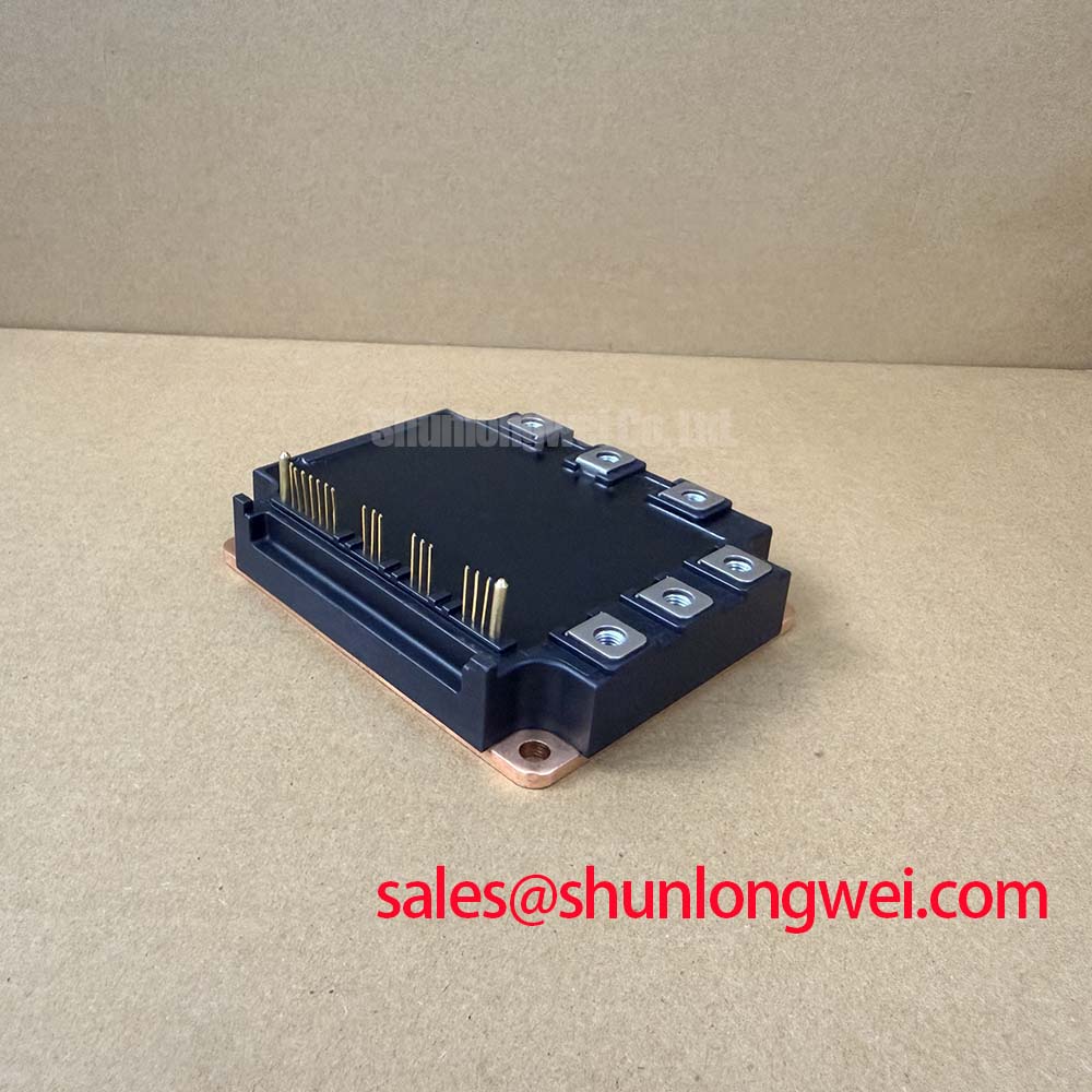
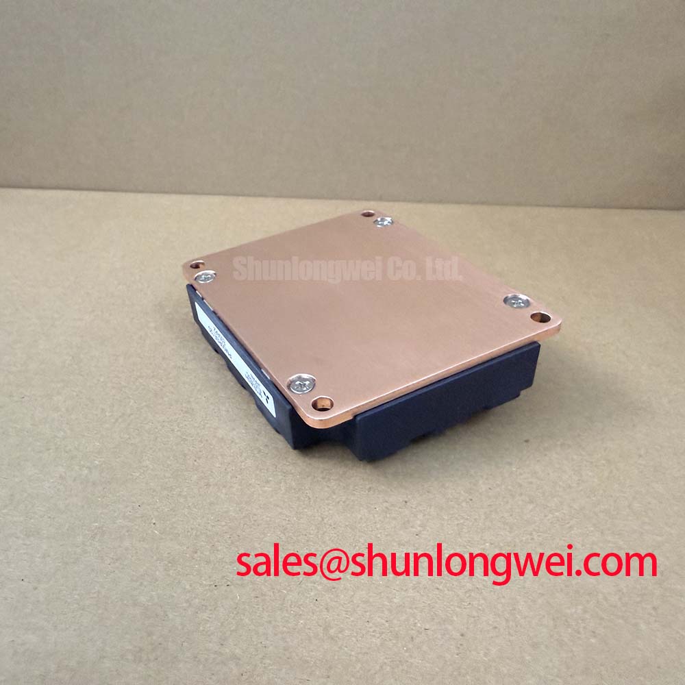
The Mitsubishi PM50RSE120 is an intelligent power module intended for high voltage switching applications that require an inverter section and an integrated brake section. Its official ratings specify a 1200 V collector emitter voltage for both sections. The inverter collector current rating is 50 A, while the brake collector current rating is 15 A. These values must be interpreted together with switching frequency, current waveform, cooling conditions, gate drive behavior, and the equipment manufacturer’s electrical limits.
| Parameter | Inverter Rating | Brake Rating | Unit |
|---|---|---|---|
| Collector emitter voltage, VCES | 1200 | 1200 | V |
| Collector current, IC | 50 | 15 | A |
| Collector emitter saturation voltage, VCE(sat), listed | 2.8 | 2.8 | V |
| Emitter collector voltage, VEC, listed | 2.5 | Not specified | V |
| Junction to case thermal resistance, Rth(j-c) | 0.38 | 1.33 | °C/W |
| Isolation voltage, AC for 1 minute, VISO | 2500 | Applicable module value | Vrms |
The listed VCE(sat) values are electrical characteristics rather than a universal operating limit for every current, temperature, or gate-drive condition. When evaluating a failed installation, compare the measured waveform and operating temperature with the original equipment documentation. A replacement assessment should also confirm terminal arrangement, mechanical interface, gate-drive compatibility, protection circuitry, and the cooling path.
PM50RSE120 Circuit Protection & Reliability: Calibrating Desaturation Detection
Desaturation protection is a system-level method for identifying an abnormal rise in the conducting device voltage during a commanded turn-on. For this module, the listed VCE(sat) value of 2.8 V provides a reference point for normal conduction assessment, but the protection threshold must not be copied directly from that listed value. The gate driver, sensing network, blanking behavior, temperature, stray inductance, and current transition all influence the voltage seen by the protection circuit.
A practical service investigation begins with the gate command and the collector emitter waveform observed together through suitably rated, isolated measurement equipment. If the protection circuit trips during a healthy switching event, engineers should check whether the sensing path is responding to a legitimate overcurrent condition, a switching transient, a noisy reference, or an incorrectly coordinated blanking interval. If the module does not turn off during a controlled fault test, the complete protection chain requires review, including the sensor path, gate driver supply, fault latch, isolation barrier, and shutdown logic.
Short circuit withstand behavior is application dependent. The supplied product information does not establish a universal short circuit safe operating time for every gate driver and circuit layout, so a specific microsecond guarantee should not be assigned to the module without the applicable Mitsubishi documentation and test conditions. The design objective is to detect the abnormal conduction state promptly, then reduce gate current in a controlled manner so that the device does not experience an unnecessary inductive voltage overshoot.
Two-stage soft turn-off is an engineering recommendation for systems where a hard gate discharge could create excessive di/dt and collector emitter overshoot. The first stage can reduce the fault current transition, while the second stage completes the gate shutdown after the switching node has been controlled. The exact timing and current profile are determined by the driver and power-loop design. Engineers should validate the sequence with a controlled double-pulse or fault-injection test while monitoring the collector emitter peak, gate voltage, driver supply, and fault response.
Gate-loop routing should remain short, symmetrical, and physically separated from high-current commutation paths. The module’s isolation voltage rating is 2500 Vrms for one minute according to the supplied official specification, but this rating does not by itself establish the creepage, clearance, pollution degree, or complete equipment insulation system. Those requirements belong to the finished assembly and must be checked against the applicable safety standard.
PM50RSE120 Thermal-Electrical Optimization: Thermal Time Constants and Peak Junction Practical Tuning
The official junction to case thermal resistance is 0.38 °C/W for the inverter section and 1.33 °C/W for the brake section. The difference is important when an energy storage inverter uses the brake circuit intermittently but at high pulse power. A heatsink selected only from the continuous inverter current may not provide the required transient thermal response for the brake duty cycle.
For pulsed operation, a steady-state Rth(j-c) value is not sufficient to describe the complete thermal event. An engineering calculation normally combines the semiconductor power waveform with the transient thermal impedance Zth(j-c) supplied in the relevant manufacturer data. The resulting junction temperature estimate must include case temperature, interface resistance, heatsink response, airflow, mounting condition, and the actual duration and repetition of the pulse. If a complete transient thermal curve is unavailable, the calculation should be treated as incomplete rather than replaced with an assumed thermal time constant.
The VCE(sat) characteristic should be measured under defined current, gate-drive, and temperature conditions. A higher measured saturation voltage may reflect increased junction temperature, insufficient gate drive, wiring impedance, current imbalance, or a damaged power path. A lower value during one test does not prove that the module is suitable for all load conditions. Oscilloscope measurements should be correlated with current-probe data and case-temperature readings so that electrical loss is not confused with a measurement artifact.
When integrating the module into a commercial string inverter or micro-grid energy storage converter, designers should examine the complete thermal path from semiconductor junction to case, interface material, heatsink, enclosure, and ambient environment. The module’s official thermal values describe the junction-to-case portion only. They do not specify the finished system temperature, allowable overload duration, or service life.
Protection timing should also be coordinated with thermal behavior. A desaturation event and a thermal overload event are different conditions: one may occur during a rapid fault transition, while the other develops through accumulated conduction and switching losses. The controller should distinguish these responses where the equipment architecture requires it, and the final thresholds should be verified during normal load cycling, regenerative events, and braking operation.
💡 Pro Tip: Record gate voltage, collector emitter voltage, current, case temperature, and fault timing on the same test run so that thermal and switching observations can be compared without relying on a single symptom.
PM50RSE120 Circuit Protection & Reliability: Calibrating Thermal Feedback
In a multi-device power stage, the positive temperature behavior of VCE(sat) can support static current sharing under suitable operating conditions. As conduction characteristics change with temperature, current distribution may move toward a more balanced state, but this effect is not an automatic guarantee of dynamic current sharing. Gate-drive delay, common emitter impedance, commutation inductance, busbar geometry, and driver output impedance can dominate the current split during fast transitions.
Parallel operation should therefore be assessed from measured current waveforms rather than from the listed saturation voltage alone. The gate paths should use matched routing and comparable impedance, with the power bus arranged so that each device sees a similar electrical path. Shared control references should be reviewed for ground bounce and common-mode disturbance. Where negative turn-off bias is considered, the system integrator must verify the permissible gate emitter voltage from the original Mitsubishi documentation and the installed driver design instead of assuming a generic value.
Gate-emitter protection is particularly important in a noisy inverter. A local gate-emitter clamp may help control unwanted excursions, but its selection, location, pulse capability, and interaction with the driver must be evaluated as one circuit. A gate signal that appears correct at the driver output may differ at the module terminal because of common-mode ground movement and parasitic inductance. Measurements should be taken at the actual module gate and emitter reference points using a probe arrangement appropriate for the switching environment.
For troubleshooting, compare the suspected phase with a known-good phase under the same low-energy test condition. Check gate amplitude, turn-on and turn-off delay, collector current symmetry, saturation voltage, and fault feedback. An abnormal difference may indicate a driver mismatch, a connection problem, a thermal imbalance, or a power semiconductor issue; the measurement sequence should be expanded before assigning a single cause.
The brake section deserves separate attention because its official collector current rating is 15 A, lower than the inverter section’s 50 A rating, and its listed junction-to-case thermal resistance is 1.33 °C/W. Brake resistor selection, regeneration control, pulse repetition, and enclosure heat removal must be verified at the system level. A brake path that is electrically within its current rating can still create an unsuitable thermal cycle if its pulse energy and repetition are not evaluated together.
For comparison work, engineers may review the objectively stated specifications of CM50DY-28H as a separate Mitsubishi power module. Similar voltage or current labels do not establish interchangeability. Terminal layout, internal topology, gate-drive requirements, thermal interface, protection behavior, and mechanical dimensions must all be confirmed from the relevant documentation before any substitution assessment.
Assembly Integrity & Layout Architecture: Implementing DC Bus Operating Voltage Headroom Derating for PM50RSE120
The 1200 V VCES rating defines an official device boundary, not a recommended DC-link operating voltage for every converter. The usable voltage headroom depends on switching overshoot, busbar inductance, commutation behavior, control response, fault energy, temperature, and the equipment’s required reliability target. Engineers should minimize the high-current commutation loop and verify the actual collector emitter peak during switching tests rather than infer it from the nominal bus voltage.
Altitude, environmental contamination, humidity, and enclosure construction can affect the insulation system and cooling performance. The supplied product data does not provide a universal altitude derating curve, cosmic-ray failure rate, single-event burnout FIT value, or operating-life prediction for this model. Such values must not be calculated from the voltage rating alone. For installations above a specified site elevation, the system designer should consult the applicable Mitsubishi application data and the relevant equipment insulation and environmental requirements, then validate the finished assembly.
Mechanical assembly is part of electrical reliability. The case must sit flat against a suitable thermal interface, fasteners should be tightened according to the module and heatsink manufacturer’s documented method, and the busbar should not impose bending stress on the terminals. Surface contamination, loose connections, and unsupported heavy conductors can create additional electrical and thermal variation. After assembly, inspect for unwanted contact, verify isolation with an approved test method, and repeat the electrical checks after thermal cycling where the service procedure allows.
For a commercial string inverter or micro-grid energy storage system, the DC-link test should include startup, steady load, regenerative transitions, braking, and controlled shutdown. The measurement plan should capture the switching-node peak, gate behavior, current sharing, and fault response at the most demanding validated operating point. Protection thresholds should be reviewed against measured behavior, while the final voltage margin remains a system engineering decision rather than a generic percentage applied to the module.
Thermal management references can be broadened through The Advanced Thermal Management Revolution, particularly when comparing insulated substrates, conventional heatsinking, and double-sided cooling concepts at the equipment architecture level. This technical context should complement, not replace, the Mitsubishi data applicable to PM50RSE120.
Gate-driver sequencing and high-side supply behavior also require verification in the finished converter. The Mitsubishi DIPIPM™ Bootstrap Circuit Design application note provides relevant background for bootstrap-based driver considerations, while the Mitsubishi Electric Diode Modules Lineup offers broader manufacturer technical context. These references do not confirm that every circuit shown is directly applicable to this module, so the original PM50RSE120 documentation and the equipment schematic remain the controlling sources.