Content last revised on September 12, 2026
2MBI50L-120 Operational Boundaries: Evaluating DC-Link Capacitance Bank Layout and Low-ES Limits
When this module is evaluated in an inverter welder or induction heating power stage, begin with the DC-link structure rather than the IGBT alone. Inspect the physical relationship between the capacitor bank, switching terminals, and current-return path. A long or asymmetric connection can add stray inductance to the commutation loop, causing a turn-off voltage overshoot that is not visible from the nominal DC-link reading.
As an Engineering Recommendation, the switching loop should be kept compact, with the forward and return conductors arranged closely and symmetrically. Laminated busbars or a carefully arranged planar conductor structure can reduce loop area. The suitable clearance and insulation system remain system-determined and must be checked against the working voltage, pollution environment, enclosure design, and applicable safety requirements. Do not infer a safe clearance from the module package alone.
The peak collector-emitter stress can be assessed by considering the DC-link voltage together with the inductive term created by stray inductance and the instantaneous current change. This relationship is an Engineering Calculation framework, not an additional factory rating for the 2MBI50L-120. During switching tests, engineers should measure the actual collector-emitter waveform at the module terminals with a properly rated differential probe. Probe-ground lead inductance can create a false overshoot and should not be treated as a reliable measurement path.
Low-ESR capacitors can improve the local high-frequency current path, but the capacitor bank must be selected as part of the complete control loop. Designers should verify ripple current, self-heating, voltage margin, discharge behavior, and the connection inductance under the intended duty cycle. Snubber capacitance and resistance should be established from measured switching waveforms and device losses rather than copied from an unrelated module family.
For maintenance work, compare the suspect assembly with a known-good power stage where available. Record the DC-link voltage, gate signal, collector-emitter waveform, current rise and fall behavior, and temperature response under controlled conditions. A waveform that changes substantially after replacing busbar hardware, capacitor connections, or probe placement may indicate a layout or measurement issue rather than a defective semiconductor.
Transient Dynamics & Electrical Design: High-Speed Fault Management: VCE Desaturation on 2MBI50L-120
The provided product data does not specify a desaturation response time, short-circuit safe operating area, gate charge, gate-emitter voltage range, or recommended gate resistance for this model. Those values must be taken from the applicable Fuji Electric documentation before a protection circuit is finalized. It would be unsafe to assign a universal detection window or gate-drive voltage to the 2MBI50L-120 from the model number alone.
For a repair evaluation, first confirm the polarity and continuity of the gate-drive wiring against the original circuit diagram. A floating gate, an interrupted return path, or an incorrectly referenced high-side driver can produce abnormal collector-emitter behavior without proving that the IGBT die has failed. The gate-emitter path should be checked with the module fully isolated and discharged, using a controlled low-energy instrument and ESD precautions.
Desaturation protection is a Design Consideration for detecting a condition in which collector-emitter voltage remains abnormally high while the control circuit is commanding conduction. The protection circuit should include suitable blanking, noise immunity, fault latching, and a controlled turn-off sequence. The required timing is system-determined by the driver, wiring inductance, load current, fault energy, and the module’s documented short-circuit limits.
A two-stage soft turn-off strategy can be evaluated where a direct gate shutdown would create excessive inductive voltage. The first stage reduces gate drive in a controlled manner, while the second stage completes turn-off after the protection circuit has confirmed the fault response. This is an Engineering Recommendation for system development, not an Official Specification of the device. Peak voltage must be verified at the module terminals during fault testing with an appropriate test fixture.
High-side driver power integrity also requires attention. If an isolated or bootstrap supply is used, the capacitor selection must account for driver quiescent current, gate-drive charge, switching frequency, leakage, start-up conditions, and allowable supply ripple. The system integrator should calculate the required capacitance from the actual driver data and measured gate-drive demand. The 2MBI50L-120 product data supplied here does not define a bootstrap capacitor value.
The Precision Gate Drive Design reference can be used as an application-level resource when reviewing gate-loop symmetry, fault timing, and switching waveform measurement. For product-family context, engineers may also consult Fuji Electric’s Fuji Electric Brake Chopper IGBT Modules page, while recognizing that information for another product family should not be transferred to this model without verification.
💡 Bench Tip: Keep the module electrically isolated, use ESD protection, and compare cold-state measurements with a known-good unit before applying any powered gate signal.
2MBI50L-120 Circuit Protection & Reliability: Calibrating Dynamic Braking Chopper Operation
In an inverter system, a braking chopper manages regenerative energy when the motor or driven mechanism decelerates and the DC link begins to rise. Whether the 2MBI50L-120 is suitable for that position depends on the actual DC-link voltage, braking current, pulse duration, repetition pattern, cooling path, and documented switching limits. The available product data confirms 1200.0 V rated voltage and 50.0 A rated current, but it does not provide a braking-energy profile or a guaranteed chopper duty cycle.
When assessing a replacement, measure the DC-link waveform during the complete deceleration event rather than checking only the steady-state bus voltage. The ballast resistor must be evaluated for instantaneous pulse energy, average thermal loading, resistance change with temperature, insulation, and fault behavior. The resistor and IGBT form one protection function, so selecting either component without considering the other can leave the DC link exposed to excessive transient stress.
As a Design Consideration, the braking threshold should be coordinated with the DC-link capacitor rating, motor controller limits, braking resistor characteristics, and the response of the supervisory fault circuit. The turn-on threshold, hysteresis, and pulse modulation strategy are system-determined. Engineers should validate the complete sequence with a current probe and isolated voltage measurement while monitoring the module case and heatsink temperatures.
Inspect the freewheel and commutation paths around the braking circuit. A diode with unsuitable reverse-recovery behavior can increase voltage ringing, switching loss, and conducted or radiated interference. The reverse-recovery softness factor is a characteristic of the selected diode and circuit conditions, not a specified attribute of the 2MBI50L-120. Any EMC evaluation belongs to the complete equipment; the module itself must not be represented as independently certified to an equipment-level EMC standard.
For a field fault, record whether the braking event is absent, intermittent, or accompanied by a protective trip, then check the command signal, gate supply, current feedback, resistor temperature, and DC-link sensing chain. These observations can help separate a control fault, an open braking path, an unsuitable energy rating, or a switching waveform problem. They do not establish a single cause without circuit-level measurements.
The 2MBI400TB-060-01 may be reviewed as a related component in a broader power topology, including upstream or auxiliary switching duties. It should be treated as a separate device for electrical verification, thermal analysis, pin assignment, and protection coordination; no substitution conclusion should be made from family naming alone.
Assembly Integrity & Layout Architecture: Implementing Static and Dynamic Current Distribution for 2MBI50L-120
Before installation, confirm the terminal identity from the original Fuji Electric documentation and the equipment wiring diagram. The supplied product information does not provide a detailed terminal map, internal circuit arrangement, dimensions, mounting-hole pattern, isolation rating, or torque specification. Those details must be verified from the correct drawing before fabrication or service replacement.
For parallel current paths, static sharing is influenced by the temperature coefficient of the conduction voltage, semiconductor tolerances, busbar resistance, and thermal coupling. A positive conduction-voltage temperature coefficient can support current balancing under particular operating conditions, but it is not a standalone guarantee of equal current. Designers should measure current in each branch under representative load and temperature conditions before approving parallel operation.
Dynamic sharing is more sensitive to gate-loop impedance and switching-path symmetry. Use matched conductor lengths and equivalent return paths where the circuit requires parallel devices. Keep power commutation conductors separate from sensitive control wiring, and minimize the loop area that carries rapidly changing current. The final arrangement must be checked with oscilloscope measurements because mechanical symmetry does not always produce identical electrical impedance.
Thermal assembly also deserves a direct inspection. The heatsink contact surface should be clean and flat, the interface material should be applied consistently, and the mounting sequence should avoid tilting the module. Designers should verify the required mounting hardware, torque, insulation washer arrangement, and creepage conditions from the manufacturer’s mechanical documentation and the equipment safety design.
Thermal cycling in bidirectional DC-DC battery systems can be affected by current ripple, switching loss, cooling transients, and repeated charge and discharge transitions. The 2MBI50L-120 should therefore be evaluated against the actual junction-temperature swing and load profile rather than a nominal current value alone. No field lifetime or cycle-life figure is established by the product data supplied here, so service planning should rely on measured thermal behavior and documented qualification data.
High-altitude cosmic-ray effects, single-event burnout, FIT rate, insulation reliability, and service life require device-specific qualification data and system conditions. The available specifications do not support a numerical claim in these areas. Engineers working at elevated altitude should obtain the applicable reliability guidance and perform a system-level risk assessment rather than applying an assumed derating factor.
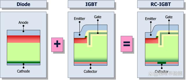
For application context, Fuji Electric’s Fuji Electric RC-IGBT Modules page provides information about a different module technology. It may help engineers understand the range of available power-module architectures, but its electrical ratings and internal configuration must not be used as specifications for the 2MBI50L-120.
During final commissioning, verify gate polarity, isolated control supply behavior, DC-link precharge, current-sensor polarity, protective interlocks, and switching waveforms at reduced system stress before proceeding to the intended operating condition. The product remains identified by its official supplied ratings of 1200.0 V, 50.0 A, and Module package; all additional operating limits must be confirmed from the applicable manufacturer documentation and validated in the completed equipment.