
Content last revised on September 10, 2026
Engineering Assessment: CM50DY-28H Dual IGBT Module Architecture
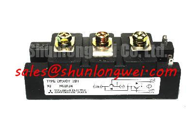
The CM50DY-28H is a dual half-bridge IGBT module developed by Mitsubishi Electric, rated at an absolute maximum collector-emitter breakdown voltage of VCES = 1400V (Official Datasheet Specification) with a continuous direct collector current of IC = 50A at a case temperature of 25°C. Built to serve harsh industrial operating conditions, this module is commonly deployed in heavy-duty variable frequency AC motor drives (VFD), uninterrupted power systems (UPS), and regenerative industrial braking stages where transient line voltages exceed the safety margins provided by standard 1200V-class silicon.
| Parameter Description | Symbol | Official Datasheet Value | Engineering Test Conditions |
|---|---|---|---|
| Collector-Emitter Voltage | VCES | 1400V | VGE = 0V (G-E Short) |
| Continuous Collector Current | IC | 50A | TC = 25°C |
| Peak Collector Current | ICM | 100A | Pulse width duration limited by maximum Tj |
| Maximum Collector Dissipation | PC | 400W | TC = 25°C, per single IGBT stage |
| Collector-Emitter Saturation Voltage | VCE(sat) | 3.1V (Typ) / 4.2V (Max) | IC = 50A, VGE = 15V |
| Gate-Emitter Threshold Voltage | VGE(th) | 5.0V (Min) / 6.5V (Typ) / 8.0V (Max) | IC = 5.0mA, VCE = 10V |
| Input Capacitance | Cies | 10nF (Max) | VCE = 10V, VGE = 0V |
| Thermal Resistance (IGBT) | Rth(j-c) | 0.31 °C/W (Max) | Per IGBT device chip |
| Thermal Resistance (Diode) | Rth(j-c) | 0.70 °C/W (Max) | Per inverse free-wheeling diode (FWDi) |
| Isolation Voltage | Viso | 2500Vrms | AC 1 minute, terminals to copper baseplate |
Optimizing Heatsink Contact Pressure and Surface Roughness for Minimum R_th(c-s)
Thermal management in heavy-duty motor drive inverters relies on minimizing the case-to-heatsink contact thermal resistance Rth(c-s) to prevent channel thermal runaway under repetitive mechanical shock loads. The module features an internal thermal resistance of Rth(j-c) = 0.31 °C/W for each IGBT switch and 0.70 °C/W for the accompanying antiparallel fast-recovery diode. However, interface degradation between the nickel-plated copper baseplate and the extruded aluminum heatsink often represents the largest bottleneck in field installations.
To establish uniform heat flux, the heatsink mounting surface must meet a flatness specification of less than 50 µm over a 100 mm span, with a surface roughness profile not exceeding Rz 12 µm. When applying thermal interface material (TIM), screen printing or roller application should maintain a controlled layer thickness between 50 µm and 80 µm. Excessive grease increases interfacial thermal resistance, while inadequate application leaves microscopic air voids that severely degrade thermal conduction.
Mechanical mounting requires a calibrated cross-pattern torque sequence to prevent baseplate deformation. Fasteners should first be hand-tightened to a pre-torque of approximately 0.5 to 1.0 N·m, followed by a final tightening to 2.5–3.5 N·m (General Industry Design Consideration for standard M5 hardware). This progressive loading allows the viscous thermal grease to displace trapped air pockets evenly outward toward the perimeter edges.
PCB Symmetry Considerations for Dual IGBT Half-Bridge Switching Paths
In high-di/dt converter topologies, asymmetrical parasitic board layout inductances lead to dynamic current imbalances, ringing, and localized dielectric breakdown. The CM50DY-28H provides dedicated auxiliary Kelvin emitter terminals for both upper and lower switches. System designers must route the gate drive signal and its corresponding auxiliary emitter return directly as tightly coupled twisted pairs or differential PCB strip lines, strictly isolated from the high-current DC-bus power return path.
If the main emitter output trace shares common impedance with the auxiliary Kelvin path, high di/dt surges induce a counter-electromotive force into the gate-emitter loop. This parasitic feedback reduces the effective turn-on gate voltage, lengthening switching transition times and driving up collector power dissipation. For industrial high-power platforms requiring higher phase currents beyond the 50A envelope of this module, the related CM200DY-24E provides a continuous collector current rating of 200A at 1200V.
💡 Pro Tip: To suppress parasitic LC oscillations driven by the internal maximum gate capacitance of Cies = 10nF, position the external series gate resistor (RG) and bidirectional transient voltage suppressor (TVS) diodes as close as physically possible to the module pin terminals. A suggested initial gate damping resistance of 10 Ω (Typical Starting Point for bench tuning) provides a balanced starting profile between switching transition losses and overshoot suppression.
Fault-Clearing Dynamics: Type-I/II Desaturation Detection and Inductive Clamping
Heavy-duty industrial motors are prone to direct phase-to-phase shorts, ground faults, and mechanical rotor lock conditions. These severe events push power modules directly into desaturation, causing current to rise rapidly while VCE climbs towards the full DC bus potential. The CM50DY-28H operates safely within its short-circuit safe operating area (SCSOA) provided the fault is detected and extinguished within a duration under 10 µs.
Hardware-level desaturation (DESAT) sensing circuits continuously monitor the collector-emitter voltage drop across the switch during the conductive on-state. Because the typical saturation voltage is VCE(sat) = 3.1V (reaching up to 4.2V at full load), the threshold comparator reference is commonly configured at 6.5V to 7.5V. When diagnosing field failures, consulting systematic testing methods outlined in the Field Engineer’s Handbook helps verify whether catastrophic switch failures originated from overcurrent-induced bond-wire lift or thermal fatigue.
Executing an instantaneous, abrupt gate shut-off during a heavy short-circuit event generates severe inductive flyback spikes due to residual DC-bus loop inductance. To prevent exceeding the absolute rating of VCES = 1400V, the gate driver must deploy two-stage soft turn-off (2STO) or active analog clamping. These protection circuits temporarily pull down the gate voltage to an intermediate level, slowing current fall rates (di/dt) and clamping transient overshoot safely within the boundaries defined by standard ROHM Transistor Safe Operating Area (SOA) Application guidelines.
Optocoupler vs Digital Coreless Transformer Isolation in High-Voltage Switching
Industrial motor drives operating on 400V/480V three-phase lines present extreme ground potential shifts during high-speed inverter transitions. Isolating the low-voltage control digital signal processor (DSP) from high-potential floating half-bridge gates requires robust galvanic isolation with a minimum isolation test rating of Viso = 2500Vrms.
While traditional high-speed optocouplers deliver dependable electrical isolation, their internal light-emitting diodes experience propagation delay drift over thermal aging cycles. In contrast, modern digital coreless transformer isolators offer transient immunity (CMTI) exceeding 100 kV/µs. This high CMTI prevents common-mode noise generated during fast switching edges from injecting transient false pulses into the gate driver logic.
Given the gate-emitter threshold characteristics of VGE(th) = 5.0V to 8.0V on the CM50DY-28H, driver stages should utilize a bipolar gate drive supply (+15V for hard turn-on saturation and -5V to -8V for negative off-state bias). Implementing negative gate bias alongside active Miller clamp circuitry completely neutralizes parasitic turn-on induced by displacement currents flowing through the collector-gate capacitance (Cres), ensuring system-level stability in industrial motor systems utilizing advanced Mitsubishi Electric CSTBT™ Technology structures.