


Content last revised on September 14, 2026
Preventing Spurious Faults: Planar Symmetrical Busbar Geometry: Practical Guidelines for SKIIP603GB172CT
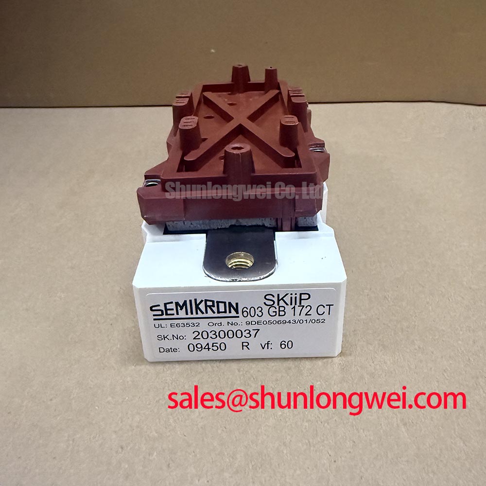
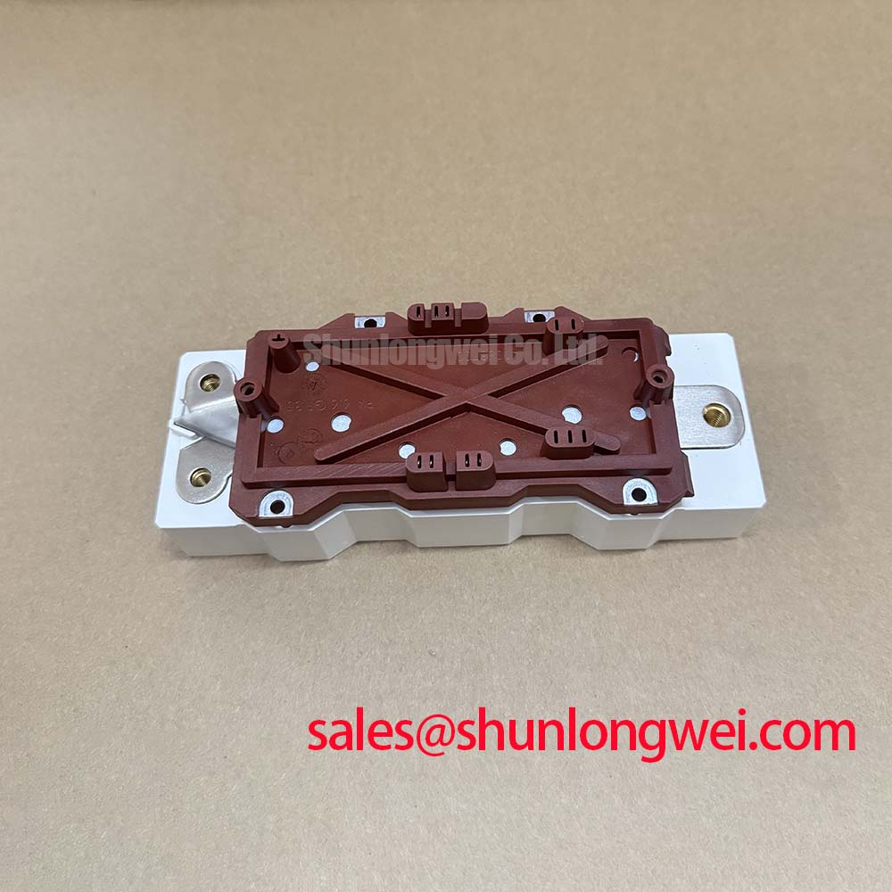
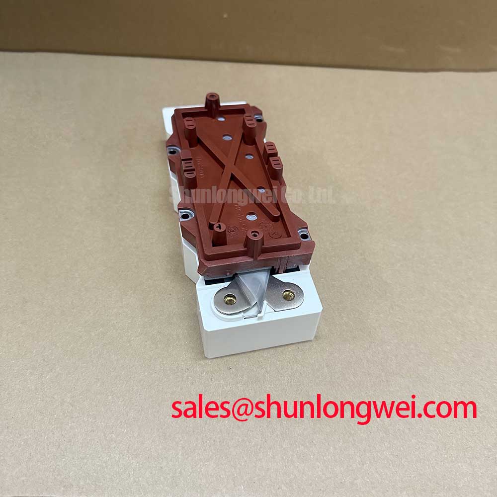
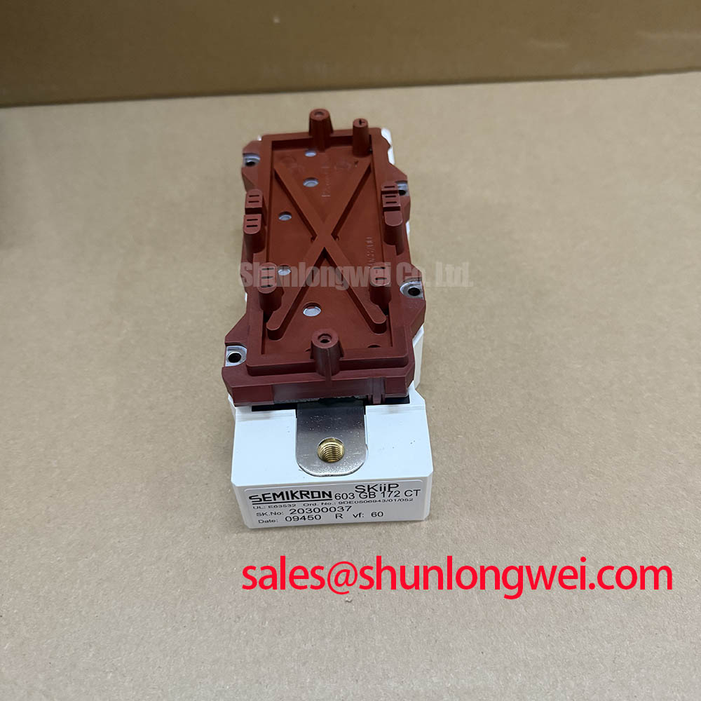
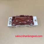
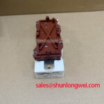
Before connecting a replacement unit, isolate the DC link, inspect the power terminals and mounting face for mechanical damage, then verify that the cabinet documentation identifies SKIIP603GB172CT as the installed Semikron power module. Cold-state multimeter checks can help identify an obvious collector-to-emitter short or unintended gate-to-emitter continuity, but they cannot confirm switching behavior, insulation condition under voltage, or the performance of surrounding drive and protection circuits.
The SKIIP603GB172CT is specified with a 1700 V collector-emitter voltage, 600 A nominal DC collector current, and 850 A collector current at Ts = 25°C. Its official limits also include ±20 V gate-emitter voltage, 10 µs short-circuit withstand time, 0.045 K/W junction-to-heatsink thermal resistance for the IGBT, an operating junction-temperature range of −40 to +150°C, and 4000 V AC isolation for one minute. These values are official datasheet specifications and should be checked against the original inverter architecture before energizing a repaired assembly.
| Official specification | Value |
|---|---|
| Collector-emitter voltage, VCES | 1700 V |
| Continuous DC collector current, ICnom | 600 A |
| Collector current at Ts = 25°C | 850 A |
| Gate-emitter voltage, VGES | ±20 V |
| Short-circuit withstand time, tsc | 10 µs |
| IGBT thermal resistance, junction to heatsink | 0.045 K/W |
| Operating junction temperature | −40 to +150°C |
| Isolation voltage | 4000 V AC, 1 minute |
When a high-power inverter trips during turn-off, begin at the physical current loop rather than changing gate-drive parts immediately. Inspect the laminated or planar busbar path between the DC-link capacitors, the module power terminals, and the return path. Uneven conductor spacing, loose terminal hardware, displaced capacitor connections, or an added repair lead can increase loop inductance and raise the turn-off voltage peak.
The relationship explains why this matters: the switching peak is determined by the DC-link voltage plus the product of stray inductance and current-change rate. A faster interruption of high current therefore creates a larger inductive overshoot. The correct busbar inductance target, snubber arrangement, capacitor location, clearance distances, and switching speed are system-determined and must be validated using measured collector-emitter waveforms under realistic current and temperature conditions.
A planar, symmetrical busbar arrangement is a design consideration for reducing the enclosed current-loop area. Keep outgoing and return conductors close together where the mechanical design permits, and avoid adding long bypass paths between the DC-link capacitor bank and the module. Check whether replacement work has altered the original stack order of copper bars, insulation sheets, spacers, or capacitor straps. Physical symmetry is especially important where parallel current paths exist, because unequal path impedance can produce uneven dynamic loading.
For a utility-scale central photovoltaic inverter, verify that the measured DC-bus operating range remains compatible with the 1700 V VCES official rating after switching overshoot is included. The device rating is not an instruction to operate the inverter at a particular DC-bus voltage. Engineers should compare the actual peak waveform, probe method, DC-link condition, protection response, and original equipment limits before making any commissioning decision.
A snubber capacitor can reduce switching-loop stress only when its placement and parasitic inductance are appropriate to the existing topology. A capacitor added remotely may have little useful high-frequency effect. Check the original schematic and capacitor mounting arrangement before substituting parts. If a repair review also involves another Semikron module family, SKIIP37AC12T4V1 should be evaluated independently for its own electrical ratings, terminal format, driver interface, and mechanical fit; it should not be treated as an automatic replacement.
⚠️ Field Alert: Disconnect and verify discharge of the DC link before removing control or power connections, then tighten hardware only to the original equipment manufacturer’s specified torque and apply thermal interface material evenly.
SKIIP603GB172CT Operational Boundaries: Evaluating High-Altitude Cosmic Ray Induced SEB Failure Limits
The SKIIP603GB172CT has a defined 1700 V VCES rating and a −40 to +150°C operating junction-temperature range, but no unsupported field-life, cosmic-ray, altitude, or FIT estimate should be inferred from those figures. Semiconductor exposure to terrestrial neutron flux and the likelihood of single-event effects depend on site altitude, DC-bus operating point, device technology, circuit topology, temperature, switching conditions, and protection behavior. These factors require system-level assessment.
For installations at elevated altitude, including sites above 2000 m, treat cosmic-ray exposure and reduced air-cooling capability as design considerations rather than fixed failure predictions. The inverter designer should consult the original equipment environmental requirements and any applicable manufacturer qualification documentation. A repaired unit should be tested within the site-specific electrical and thermal operating envelope rather than assigned a calculated service-life claim without authoritative evidence.
Switching frequency also changes the balance between switching loss, conduction loss, heatsink performance, airflow, and control response. Where an inverter can operate across multiple switching-frequency modes, measure case temperature, coolant or airflow condition, phase current, and switching waveforms in each relevant mode. A rising heatsink temperature may result from reduced airflow, contaminated cooling channels, thermal-interface degradation, excessive switching loss, phase imbalance, or a control issue. It should not be attributed to one cause without evidence.
The module’s official 10 µs short-circuit withstand time is a fault-survival boundary, not a permitted operating pulse width or a substitute for coordinated protection. The gate-drive and controller architecture must detect and remove a fault within the actual system protection sequence. Evaluate semiconductor fuses through their published time-current and I²t documentation together with the inverter’s available fault energy and contactor behavior. Do not assume that a fuse alone can protect the module during every internal short-circuit event.
For repair teams reviewing a broader power chain, the role of an upstream or auxiliary switching stage should be documented separately. A device such as SKM100GB063D may appear elsewhere in a converter assembly, but its ratings and function must be verified against that stage’s schematic rather than inferred from proximity to the SKIIP module.
SKIIP603GB172CT Thermal-Electrical Optimization: Suppressing Cres Induced Gate Voltage Spikes Through Practical Tuning
Unexpected turn-on during commutation often requires observation at the gate-emitter terminals with a suitable differential measurement method. A high collector voltage transition can couple through the IGBT’s internal capacitances and raise the gate voltage of the device intended to remain off. If the gate loop has excessive impedance, poor return routing, a damaged clamp path, or shared control power noise, this coupled pulse can contribute to cross-conduction.
A practical recommendation is to inspect the complete off-state gate path: gate resistor network, driver output stage, gate-emitter return connection, isolation barrier, local driver supply decoupling, clamp circuit, and the physical route of the gate harness or board traces. An active Miller clamp, where provided by the original driver arrangement, should be checked as a functional circuit rather than bypassed. Negative gate bias may be used in some system designs, but its value, driver compatibility, and transient limits must be determined from the original drive specification and remain within the official ±20 V VGES limit.
Separate power-return and control-return paths where the original layout intends them to be separated. A gate-driver reference that shares a noisy high-current return path can create apparent gate voltage movement even when the controller command is correct. Compare the affected phase with a known-good phase, including probe placement and bandwidth, before modifying damping components. Changing gate resistance without checking collector overshoot, turn-off loss, noise immunity, and protection timing can trade one fault symptom for another.
No thyristor trigger current or trigger-voltage characteristic should be assigned to this IGBT power module. Parameters such as IGT and VGT belong to thyristor devices and are not applicable identifiers for the SKIIP603GB172CT. Maintenance documentation should keep the gate-drive requirements for this module separate from any thyristor-based precharge, bypass, or auxiliary circuit that may exist elsewhere in the equipment.
Semikron’s published discussion of sintering technology provides useful packaging context for engineers assessing thermal interfaces across power-module technologies. It does not replace the official thermal limits and mounting instructions applicable to this specific module.
SKIIP603GB172CT Operational Boundaries: Evaluating Thermal Capacitance Versus Heatsink Limits
Under heavy pulsed loading, a stable heatsink temperature does not prove that the semiconductor junction is stable. The thermal mass of the module and heatsink delays the temperature response, while repeated current pulses can raise junction temperature faster than a surface sensor indicates. The official 0.045 K/W Rth(j-s) value for the IGBT is a steady thermal path specification, while transient junction response depends on pulse duration, repetition, dissipation waveform, mounting condition, and the complete cooling assembly.
When evaluating overload behavior, use the manufacturer’s applicable transient thermal data if available for the original equipment design. Multi-stage thermal models can estimate the relationship between pulsed loss and junction temperature, but the calculated result remains an engineering calculation that requires verification against actual operating conditions. The allowable peak junction temperature must remain within the official +150°C operating limit, with all uncertainty from current measurement, ambient condition, cooling performance, and switching loss considered by the system engineer.
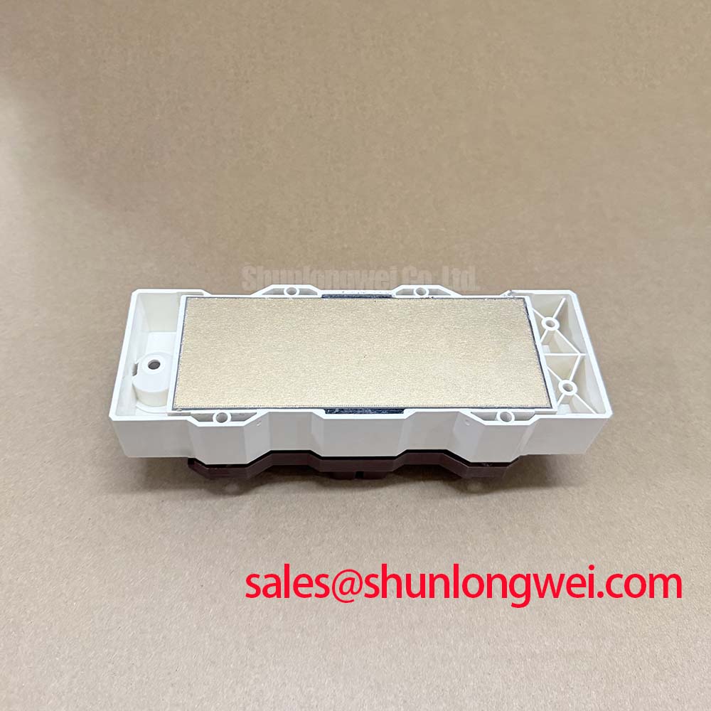
During a service inspection, examine the heatsink flatness, debris accumulation, forced-air direction, liquid-cooling flow where applicable, thermal-interface coverage, and signs of uneven clamping. Record temperature at repeatable points and compare phases under equivalent load. A phase running hotter than the others may indicate a thermal interface issue, unequal current sharing, altered switching behavior, or a measurement-location difference. Oscilloscope and thermal measurements should be correlated before replacing the module.
The official 4000 V AC isolation voltage for one minute is an isolation specification, not a universal cabinet clearance or creepage rule. Maintain the original insulation barriers, terminal covers, conductor spacing, and enclosure clearances specified by the equipment manufacturer. For practical service reference on the interaction between module packaging and cooling architecture, see The Advanced Thermal Management Revolution. Semikron’s MiniSKiiP power-module information is also relevant background when identifying differences among module platform formats and integration interfaces.