

Content last revised on September 24, 2026
SKKQ1500/18E Replacement Verification
Before fitting the SKKQ1500/18E, compare the cold terminal to terminal diode mode readings, terminal arrangement, case condition, and the host drive documentation with the removed unit while the DC link is isolated and discharged.
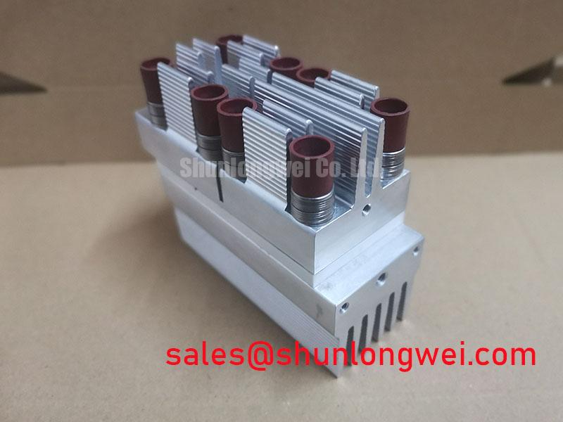
The SKKQ1500/18E is a Semikron power module supplied in the Semitrans housing format. Its declared current rating is 1500.0 A and its working voltage is identified as a Standard Industrial Rating. These are Official Specification details. The available product information does not establish a gate pin arrangement, internal circuit topology, switching ratings, short circuit withstand time, insulation rating, or individual terminal assignment. Those items must be verified against the original equipment circuit diagram and the applicable manufacturer documentation before replacement or commissioning.
| Model | SKKQ1500/18E |
| Manufacturer | Semikron |
| Current Rating | 1500.0 A Official Specification |
| Housing | Semitrans Official Specification |
| Working Voltage | Standard Industrial Rating Official Specification |
For a heavy duty variable frequency AC motor drive repair, the module should be assessed as part of a complete power stage rather than installed from current rating alone. Confirm terminal spacing, busbar orientation, heatsink interface, control board connection, protection circuit compatibility, and the electrical function of the original position. Semikron Danfoss provides broader package context through its SEMITRANS® industry standard power module information.
SKKQ1500/18E Circuit Protection & Reliability: Calibrating Fault Clearing Dynamics with Type I and Type II Desaturation
Desaturation protection is a driver level protection function, not a published standalone performance specification of the SKKQ1500/18E. In a gate controlled power stage where the original circuit uses desaturation monitoring, the driver observes the controlled device voltage during conduction. An abnormal voltage rise can indicate that load current, a wiring fault, or a bridge commutation event requires protective action. Whether the existing drive classifies its response as Type I or Type II depends on the original driver architecture and fault handling sequence.
When investigating a removed module, first inspect the driver board for the desaturation sensing path, blanking network, clamp components, isolated supply condition, and gate return routing. A missing, damaged, or incorrectly connected sense path can cause nuisance trips or leave a fault inadequately managed. Engineers should also determine whether the original controller records a fault latch, retries after a controlled delay, or commands a shutdown of the complete inverter. These behaviours are system determined and should be preserved during repair.
Soft turn off is commonly used as a Design Consideration where a driver must interrupt substantial fault current without causing a sharp inductive voltage excursion. A staged gate discharge can reduce the rate of current change, but it must be validated against the connected motor cable, DC link layout, snubber network, and device safe operating limits stated in the appropriate original documentation. No short circuit withstand time is claimed here for the SKKQ1500/18E because that value is not included in the available Official Specification data.
Physical clearances around high energy terminals should be maintained according to the equipment safety design and local service procedure. Keep the sensing conductors separated from high current busbar paths where practical, since coupled noise can affect fault detection. If an inverter trips immediately under commanded switching but static checks are inconclusive, capture the gate command, device voltage sensing signal, DC link voltage, and fault output with suitable isolated measurement equipment. Compare the event with a known good phase or an approved reference waveform before attributing the issue to the power module.
💡 Bench Tip: Use ESD precautions and record cold state terminal readings before energizing the replacement assembly, because a repeatable baseline is more useful than a single pass or fail observation.
For systems being reviewed beyond conventional silicon switching arrangements, the linked Wide Bandgap Revolution technical resource helps frame why switching edge rate, isolation behaviour, and layout verification remain important at the system level.
Field Diagnostics & Commissioning: Multi Module Parallel Current Sharing in SKKQ1500/18E Topologies
Parallel operation should never be presumed simply because multiple positions use the same Semitrans housing. Before energization, establish whether the original equipment uses parallel devices, separate bridge legs, or another internal power arrangement. The 1500.0 A rating is an Official Specification for this model, but it does not by itself define permissible current sharing, pulse capability, thermal distribution, or the number of modules suitable for a specific converter.
In IGBT based parallel arrangements, the positive temperature coefficient of on state voltage can support steady state current balancing under suitable conditions. This is a Design Consideration rather than a guaranteed current sharing statement for this model. Dynamic sharing can still become uneven when gate loop path lengths, gate resistance networks, driver propagation delays, current sensing positions, or power loop geometry differ between parallel locations.
Commissioning should begin with a low risk functional check under the host equipment’s approved startup procedure. Confirm that each gate driver receives its intended command, that complementary channels remain interlocked, and that the controller applies the designed dead time. Dead time is determined by the original switching behaviour, driver delays, device characteristics, and measured commutation conditions. It should be reviewed using waveform evidence rather than altered by an arbitrary universal value.
Where oscilloscope access is available, compare current waveforms and gate emitter references across corresponding positions. A mismatch may indicate unequal busbar resistance, an asymmetric gate loop, driver output degradation, or an issue elsewhere in the load path. It does not automatically establish a defective module. Thermal observation can also provide useful comparative evidence during controlled testing, provided the service team follows the equipment’s energized work procedures.
If the existing drive uses a separate IGBT position in its control or auxiliary conversion stages, the SKM75GB07E3 can be reviewed as a related system topology component. It is not presented as an automatic substitute for the SKKQ1500/18E. Electrical function, package interface, control method, and original circuit requirements must be verified individually.
Assembly Integrity & Layout Architecture: Implementing Planar Symmetrical Busbar Geometry for SKKQ1500/18E
Start mechanical assembly by cleaning the heatsink contact area, checking for burrs or debris, and confirming that the module seats evenly without rocking. The Semitrans housing designation is an Official Specification, but mounting hardware, mounting torque, thermal interface material thickness, and heatsink flatness requirements should be taken from the relevant manufacturer documentation or the original equipment service instructions. They must not be inferred from the housing name alone.
Power loop inductance is a practical concern in high current switching assemblies. During turn off, the observed peak voltage is influenced by DC link voltage plus the voltage created by loop inductance and changing current. This relationship means that compact, paired, and symmetrical forward and return current paths can help suppress inductive overshoot. The final layout must be validated by system switching tests that verify peak voltage margins against the actual DC link and operating load.
A planar busbar approach is often evaluated where the assembly has parallel conductive planes with a close and controlled current return path. For multi module arrangements, use matched conductor length, similar cross sectional geometry, and equivalent DC link capacitor connection paths where the original mechanical architecture permits it. Do not add or resize a snubber capacitor based only on a module current marking. Snubber selection depends on measured ringing frequency, stored energy, capacitor ripple capability, existing damping components, and the complete inverter operating envelope.
Inspect each terminal connection for correct orientation, clean contact surfaces, and even clamping force. A poorly seated busbar can create local resistance and heat, while an asymmetric connection can change current distribution between parallel paths. After assembly, an insulation and continuity check should follow the host equipment’s approved test method and voltage rating. The available Official Specification information does not state an isolation test voltage for this module, so no specific dielectric withstand value should be assumed.
For a different repair position requiring an independent compatibility review, SKM100GB063D is a related Semikron module reference. Matching manufacturer family alone does not confirm functional interchangeability. Verify electrical ratings, terminal layout, control interface, mechanical dimensions, and thermal conditions against the original equipment design.
Benchtop Waveform Tuning: Mitigating Stress from High dv/dt Cross Conduction Shoot Through on SKKQ1500/18E
Before adjusting a drive board, confirm whether the original circuit includes an active Miller clamp, separate turn on and turn off paths, negative gate bias, optical isolation, or digital isolation. None of these control features is established by the listed product parameters for the SKKQ1500/18E. They belong to the surrounding driver system and must be identified from the equipment schematic, board markings, and documented controller requirements.
High dv/dt events can couple through parasitic capacitances and wiring impedance, potentially causing an unintended gate disturbance in a complementary switch position. In a bridge circuit, this can contribute to cross conduction if interlock behaviour, gate reference routing, or driver immunity is inadequate. A dedicated low impedance gate return path and properly implemented Miller clamp are common Design Considerations, particularly where the original design uses fast switching edges. Their effectiveness must be assessed from measured waveforms at the relevant gate reference point.
Negative gate bias can be part of a system specific strategy for maintaining a controlled off state, but the required value must be taken from the original gate driver and device documentation. Applying a generic negative voltage without confirming the permitted gate limits, driver supply arrangement, and clamp behaviour can introduce avoidable risk. The same restraint applies to changes in gate resistor values, bootstrap capacitor selection, and freewheel diode recovery management.
In isolated driver circuits, examine the isolation barrier supply stability, local decoupling placement, command signal integrity, and return current path during high common mode transients. A symptom such as irregular pulse width, intermittent fault indication, or unexpected gate activity may indicate coupling, timing, supply, or measurement reference issues. Use differential or isolated probes and compare the measurement with the known good control path before changing components.
Semikron Danfoss discusses integrated driver and power module concepts through its SKiiP® technology material. For the SKKQ1500/18E installation itself, retain the original drive’s verified protection logic, use documented connection practices, and confirm behaviour under controlled commissioning conditions.