




Content last revised on September 24, 2026
SKKT 40/18E Circuit Protection and Reliability: Calibrating Semiconductor Protection Fuse Selection
For a service replacement, begin with the original circuit diagram and the protection fuse coordination record rather than selecting a fuse from current rating alone. The semiconductor fuse must be assessed against the module’s permitted surge and short circuit withstand data in the applicable Semikron documentation. A suitable coordination review compares the fuse clearing energy with the module’s specified I²t limit, while also considering the prospective fault current, DC link or AC supply impedance, and the time required for the protective device to interrupt the fault.
The available product information confirms the 1800 V voltage class and 40 A current rating, but it does not provide a fuse I²t coordination table or a module I²t value here. Designers should therefore obtain the relevant manufacturer datasheet before approving a fuse. Do not treat the module’s rated current as a substitute for a semiconductor fuse coordination study.
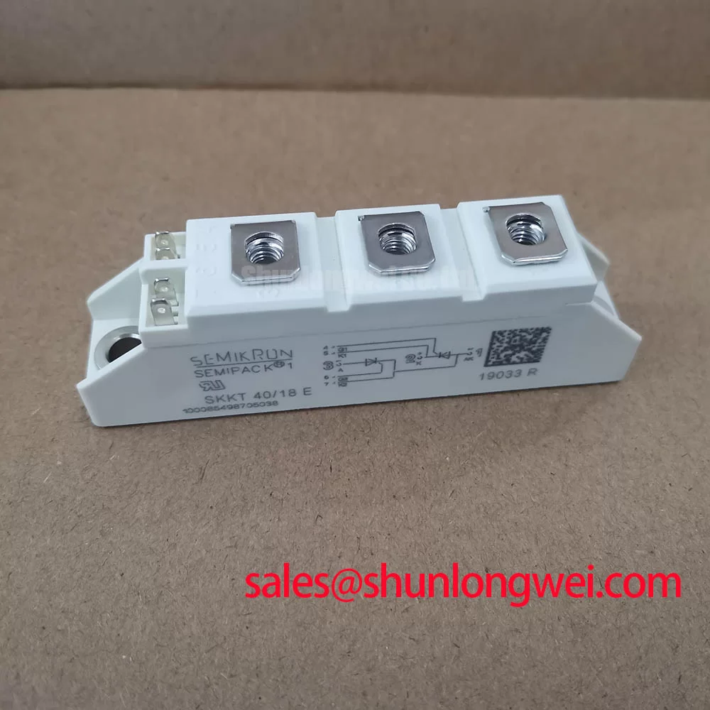
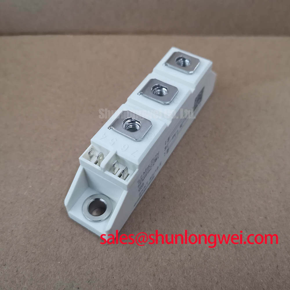
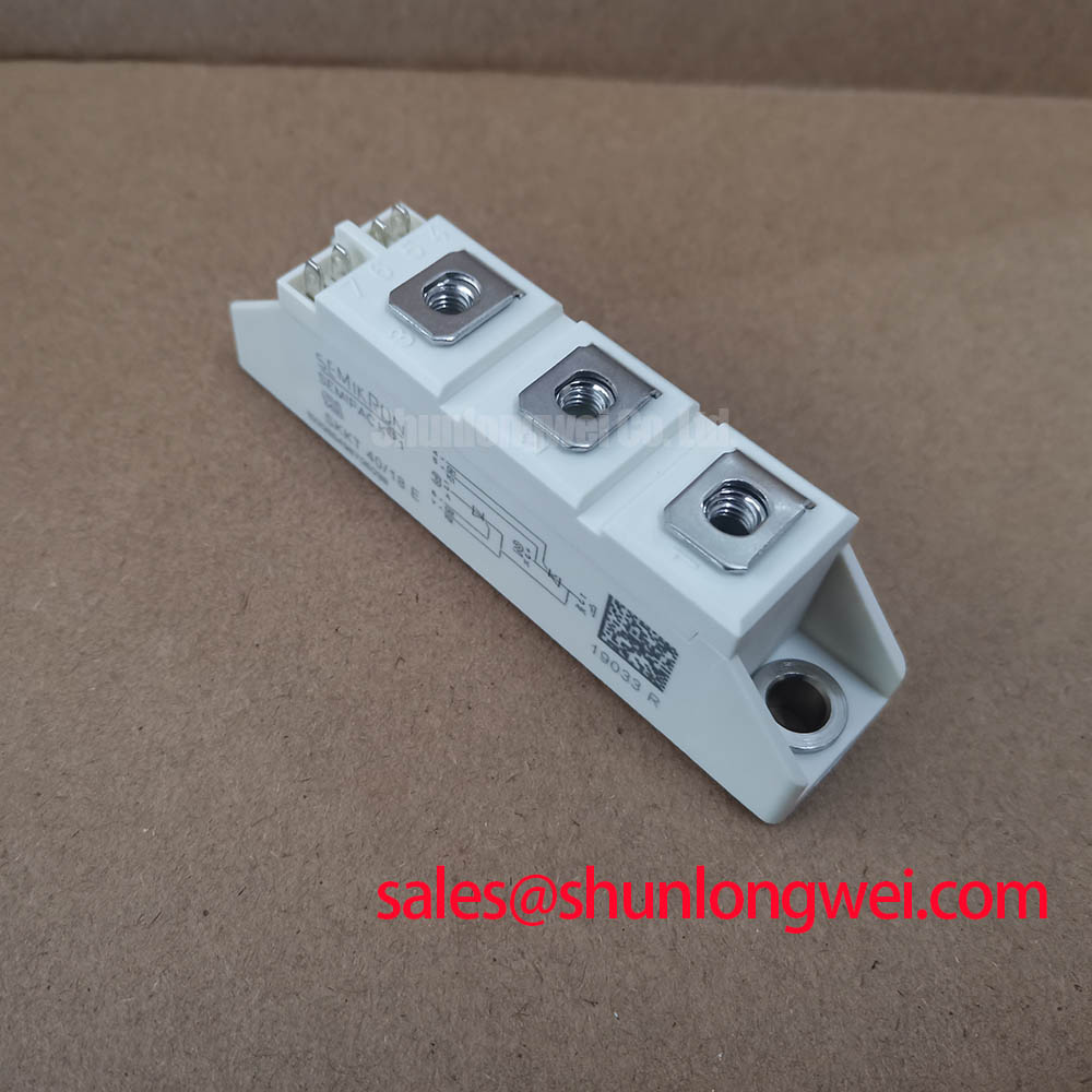
Inspect the clamping faces, terminal threads, busbar surfaces, and insulating interfaces during installation. The mounting method should follow the Semikron mechanical instructions for the Semipack housing, including the specified pressure distribution and tightening sequence. The exact mounting torque is not stated in the supplied product data and should be verified from the applicable mechanical drawing. Protective devices, MOV networks, and upstream disconnects should be selected and tested as part of the complete SVC or thyristor switched capacitor assembly.
The Semikron SEMIPACK® Thyristor / Diode Modules product information is a useful reference for package family characteristics and application documentation.
SKKT 40/18E Thermal Electrical Optimization: Gate Firing and Contact Temperature Control
Gate circuit commissioning should be performed with the module disconnected from the high energy section and with the firing board checked against the original control design. The required gate pulse amplitude, pulse width, rise time, gate current, and any back porch or repeated pulse method must come from the relevant device data and firing circuit specification. The supplied information does not confirm a gate current gradient above 1 A per microsecond, a holding current value, or a multi pulse firing requirement, so these values should not be assumed for this part.
For a grid tied static Var compensator, the control engineer should verify firing synchronisation at the intended line phase angle and observe the gate signal under the actual isolation and wiring conditions. Optocouplers or digital isolators should be checked for common mode transient behaviour appropriate to the switching environment. This is a system level design consideration, not an independent EMC or isolation certification claim for the module.
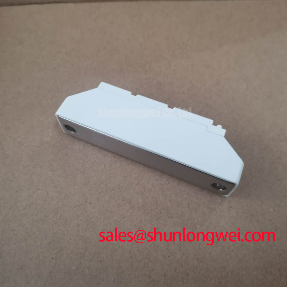
Thermal inspection should include both sides of the clamped assembly, the heatsink contact surfaces, thermal interface material condition, and airflow through the cabinet. Uneven pressure or aged interface material can create a local temperature rise even when the average load current appears acceptable. Maintenance Note: After scheduled cleaning and reassembly, monitor terminal and heatsink contact temperatures under a known operating load and recheck the cooling path for blocked airflow or condensation.
When a cross reference is required, engineers may evaluate the related SKKH273/18E as a separate device option, but electrical, mechanical, gate drive, and protection compatibility must be confirmed before any substitution.
Transient Dynamics and Electrical Design: Sinusoidal Half Cycle Surge Current
Short duration overload review should use the manufacturer’s declared ITSM rating, pulse duration, initial junction temperature, and recovery conditions. Those values are not included in the supplied parameter set, so the SKKT 40/18E’s half cycle surge capability cannot be calculated from the 1800 V and 40 A ratings alone. Before approving an SVC switching duty, designers should compare the expected sinusoidal fault or inrush current with the official surge table and confirm the thermal recovery interval before reverse voltage is reapplied.
In practical commissioning, record the switching waveform at the power terminals with suitable isolation and bandwidth. Check the peak current, voltage polarity, firing angle, and any abnormal ringing after capacitor energisation. MOV protection may be considered to control line or commutation transients, but its clamping level, energy capability, leakage, and coordination with the semiconductor fuse must be selected from the complete system voltage and fault study.
Terminal creepage and electrical clearance should be preserved during busbar installation. Keep conductive debris, loose washers, excess interface compound, and moisture away from the insulating surfaces. The enclosure design should address condensation and humidity cycling where the equipment operates in a cold start or poorly ventilated industrial environment.
For assemblies that use complementary rectification stages, the SKKH330/08E may be reviewed as a related Semikron power module reference. It should not be treated as an automatic companion or replacement without checking the circuit topology and ratings.
Field Diagnostics and Commissioning: Minimizing Commutation Turn Off Voltage Stress
During commissioning, capture the voltage across the module and the current through the commutation path at the same time. Reverse recovery peak current, recovery time, circuit stray inductance, transformer leakage, snubber condition, and line impedance all influence the observed turn off voltage. The supplied product data does not state IRRM or trr values for this part, so these characteristics must be taken from the correct Semikron technical document rather than inferred from the package name.
If the measured waveform shows excessive ringing or an unexpected voltage peak, inspect the busbar loop, terminal clamping, snubber connection, MOV condition, and gate synchronisation before attributing the result to the module. The design objective is to minimise parasitic loop inductance and verify peak voltage against the system insulation and semiconductor limits during controlled switching tests. Engineers assessing the wider failure mechanisms can consult The Ultimate IGBT Knowledge Base as a general power semiconductor engineering reference.
Final acceptance should include cold resistance and insulation checks with the circuit safely isolated, visual inspection after thermal cycling, terminal tightness verification according to the official mechanical instructions, and a controlled load test. The Semikron CAL Diode Technology page may provide broader technology context, but it does not replace the specific SKKT 40/18E datasheet for application limits.