



Content last revised on October 5, 2026
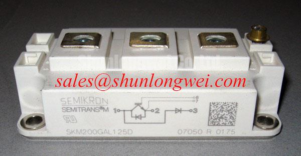
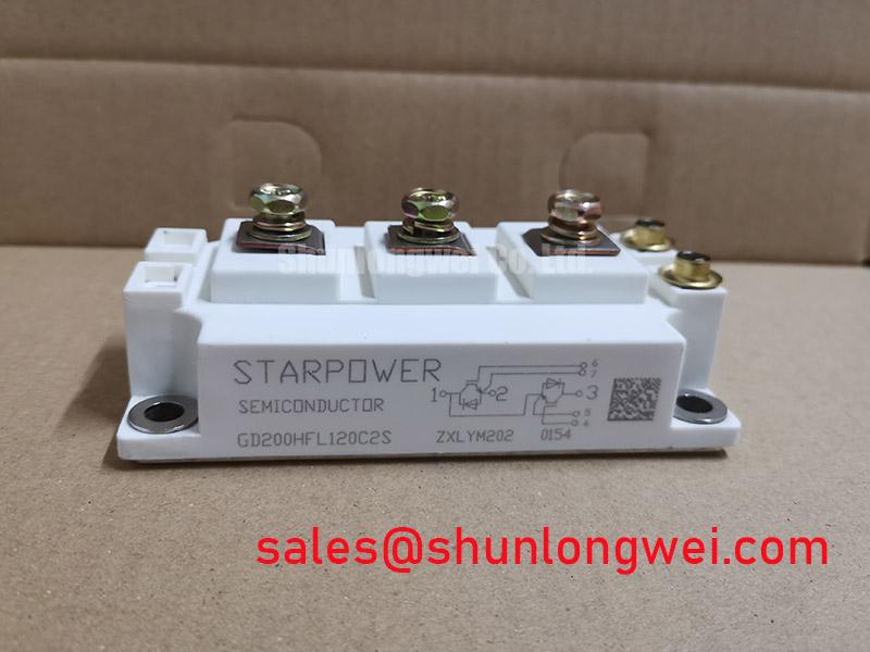
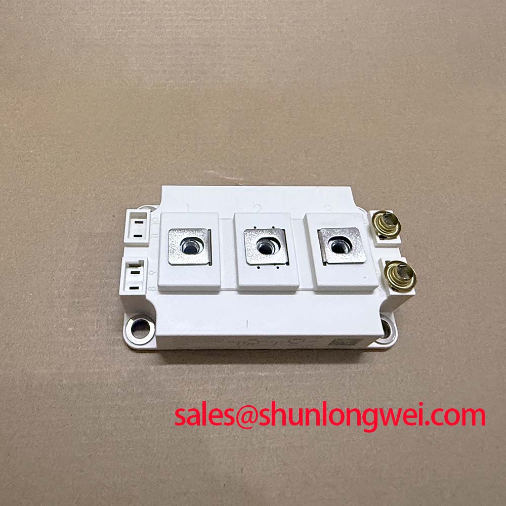
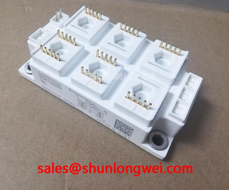
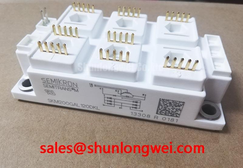
SKM200GAL1200KL Semikron 1200V 200A IGBT Module
Begin service evaluation by isolating and discharging the DC link, inspecting the Semitrans housing and terminals, and verifying the nameplate boundary of 1200.0 V voltage and 200.0 A current before any powered test. The SKM200GAL1200KL is a Semikron IGBT module in a Semitrans package. These values are Official Specification data supplied for product identification; the complete switching, thermal, isolation, gate-drive, and overload limits must be checked against the applicable manufacturer documentation before installation.
| Parameter | Published value | Engineering relevance |
|---|---|---|
| Manufacturer | Semikron | Confirm the original equipment documentation and mechanical interface before replacement evaluation. |
| Model | SKM200GAL1200KL | Use the complete ordering code when checking system records and procurement documents. |
| Rated voltage | 1200.0 V | Official Specification; verify DC-link operating and transient conditions at system level. |
| Rated current | 200.0 A | Official Specification; actual permissible current depends on switching conditions, cooling, duty cycle, and junction temperature. |
| Package | Semitrans | Mechanical mounting, terminal arrangement, creepage, clearance, and thermal interface details require confirmation from the relevant mechanical documentation. |
For device-family context, engineers can review the Semikron-Danfoss SEMITRANS® Industry Standard IGBTs reference and the broader Semikron-Danfoss Power Modules Catalog. Those references provide industry context, but they do not replace the product-specific ratings and application conditions applicable to this model.
Preventing Spurious Faults: Baseplate Thermal Grease Layer Control Guidelines for SKM200GAL1200KL
During installation, clean the heatsink surface and module baseplate with a process approved by the equipment manufacturer, then inspect both surfaces under suitable lighting. The contact area should be free from particles, burrs, dried compound, and local damage that could hold the baseplate away from the heatsink. Thermal interface material should form a continuous, controlled film rather than isolated pools or visible dry zones. The correct film thickness is system and material dependent, so the integrator should follow the TIM supplier’s application data and the module manufacturer’s mechanical instructions instead of treating a generic thickness as an SKM200GAL1200KL specification.
Baseplate flatness and heatsink rigidity deserve attention when a module is installed in a high-current converter. A curved heatsink can create local pressure concentrations, while an uneven baseplate contact can increase thermal resistance even when the fasteners appear tight. Apply the mounting hardware progressively in the specified sequence so the module seats evenly. The final tightening method, screw sequence, washer arrangement, and torque must come from the relevant mechanical documentation for the module and heatsink assembly.
When a converter reports intermittent overtemperature or gate-driver faults, inspect the thermal interface before changing electrical protection settings. Check the heatsink contact pattern, fan or liquid-cooling operation, sensor attachment, and the temperature trend during a controlled low-energy test. A thermal camera can help locate uneven heating, but its reading should be correlated with the installed sensor and the actual switching duty. A fault that appears only after several load cycles may involve thermal impedance, current imbalance, cooling airflow, or protection timing rather than a semiconductor defect alone.
Field Alert: Disconnect the DC link and gate-drive supply, and verify the DC link is discharged before touching module terminals, gate wiring, or the heatsink assembly.
Preventing Spurious Faults: DC-Link Capacitance Bank Layout and Low-ES Guidelines for SKM200GAL1200KL
The commutation loop between the DC-link capacitor, the module power terminals, and the return path should be treated as a high-frequency circuit, not simply as a low-resistance conductor. Minimize the physical loop area and keep the forward and return conductors closely coupled. Symmetrical planar busbar geometry can reduce current crowding and parasitic inductance, while the final design must be validated by measuring switching-node voltage with a properly compensated differential probe.
Turn-off overshoot is influenced by DC-link voltage, commutation current, switching speed, stray inductance, diode recovery behavior, and the impedance of the capacitor bank. The familiar relationship between peak voltage, DC-link voltage, stray inductance, and current slew rate is useful as an engineering calculation, but it does not establish a universal clamping value for this module. Designers should verify peak voltage during double-pulse or representative switching tests and compare the measured result with the applicable voltage boundary and protection strategy.
Place high-frequency decoupling close to the power terminals where the mechanical layout permits, while locating bulk energy storage according to the converter’s current ripple and control requirements. Equivalent series resistance, equivalent series inductance, ripple current capability, temperature, and capacitor ageing all affect the DC-link response. A snubber may reduce ringing when its location, impedance, pulse energy, and thermal behavior are proven by measurement; its component value should be selected from the switching waveform and loss calculation rather than copied from an unrelated inverter.
In a commercial string inverter or micro-grid energy-storage converter, long connections between the capacitor bank and power module can interact with cable inductance and busbar resonance. If the waveform contains repeated ringing, check probe grounding, capacitor placement, busbar symmetry, gate resistance, and freewheeling diode recovery behavior as a combined network. Radiated interference should be assessed at the complete equipment level. The IGBT module itself should not be described as independently holding CISPR or EN 55011 compliance.
For a related upstream or complementary topology review, the SKM100GB063D can be evaluated as a separate power-module entry in the system architecture. It should not be treated as an automatic substitute for the SKM200GAL1200KL without confirming voltage, current, switching, mechanical, thermal, and control compatibility.
Assembly Integrity & Layout Architecture: Implementing Galvanic Gate Drive Isolation for SKM200GAL1200KL
Gate-drive integration begins with the actual terminal definition and the original equipment schematic. Confirm the gate and emitter connections with the applicable Semikron documentation, then inspect the driver board for contamination, damaged insulation, loose connectors, and unintended copper paths. Galvanic isolation must be evaluated as part of the complete gate-driver assembly, including the isolator, isolated power supply, PCB spacing, connector construction, enclosure, and test method. A generic isolation voltage or common-mode transient rating must not be assigned to the module without a supporting source.
The gate loop should be compact, with the outgoing gate path and emitter return arranged to limit shared inductance. Keep power commutation paths physically separated from sensitive driver traces, and avoid routing high dv/dt switching nodes beside the isolation barrier or gate signal conductors. The gate resistor, turn-on and turn-off paths, clamp network, and driver supply decoupling should be reviewed together. Their final values and timing are system-determined and should be tuned against measured gate-emitter voltage, collector-emitter voltage, switching current, and device temperature.
Spurious turn-on can be investigated by observing the gate-emitter waveform during the opposite switch transition. A brief disturbance may result from Miller coupling, common-source or emitter inductance, driver supply movement, isolation capacitance, or an incorrect probe reference. Compare the suspect phase with a known-good phase under the same test conditions. If a short-circuit protection circuit is used, verify the desaturation detection path, soft turn-off behavior, blanking arrangement, fault latch, and reset sequence using a controlled test method. The relevant short-circuit safe operating area and VCE(sat) behavior must be taken from the manufacturer’s data rather than inferred from the nominal current rating.
For multi-device assemblies, positive temperature coefficient behavior may support static current sharing, but it does not guarantee dynamic sharing during fast switching. Differences in gate-loop inductance, driver propagation, busbar geometry, thermal coupling, and current sensor placement can still produce unequal transients. Designers should measure each branch during turn-on, turn-off, overload, and recovery conditions before approving parallel operation.
SKM200GAL1200KL Thermal-Electrical Optimization: Auxiliary Emitter Return Trace Separation Practical Tuning
Where the package provides a separate auxiliary emitter connection, treat that return as a gate-reference path rather than as a convenient extension of the main load-current conductor. The main emitter path carries substantial commutation current and can develop voltage across its parasitic inductance. If the driver reference shares that path, the gate-emitter voltage seen by the driver may differ from the voltage at the semiconductor terminals, increasing the possibility of oscillation or unintended gate modulation.
Route the auxiliary emitter return directly to the driver reference and keep it separate from the high-current emitter route until the intended connection point defined by the power topology. Avoid placing the auxiliary trace inside a loop formed by the collector or DC-link switching path. The gate and auxiliary-emitter conductors should remain closely associated, while the driver signal path should be kept away from high dv/dt copper. Final trace width, spacing, layer transition, and via arrangement are layout decisions that require oscilloscope verification.
During troubleshooting, measure gate-emitter voltage with a short, low-inductance probing arrangement and compare it with the collector-emitter waveform. Look for ringing that coincides with the opposite device switching, abnormal gate plateaus, delayed turn-off, or a difference between low-current and high-current tests. Also inspect the driver supply decoupling and isolation return because a clean auxiliary emitter layout cannot correct an unstable isolated supply or an incorrectly referenced probe.
When evaluating a mechanically related Semikron module, engineers may review SKM75GAL063D as a separate family reference. Any direct replacement decision still requires confirmation of electrical ratings, internal topology, terminal arrangement, thermal interface, gate requirements, and protection behavior. For thermal architecture background, see The Advanced Thermal Management Revolution, which discusses broader cooling concepts without changing the product-specific limits of the SKM200GAL1200KL.
For long motor cables or remote loads, the switching network should also be checked for transmission-line effects and reflected voltage. Filtering, edge-rate control, common-mode management, and cable termination are system-level measures. Their suitability should be established through measured collector-emitter voltage, motor-terminal waveform, conducted emissions, and protection response under the actual installation conditions.