


Content last revised on September 15, 2026
Preventing Spurious Faults: Short Circuit Withstand Limits and Coordination Guidelines for TT430N22KOF
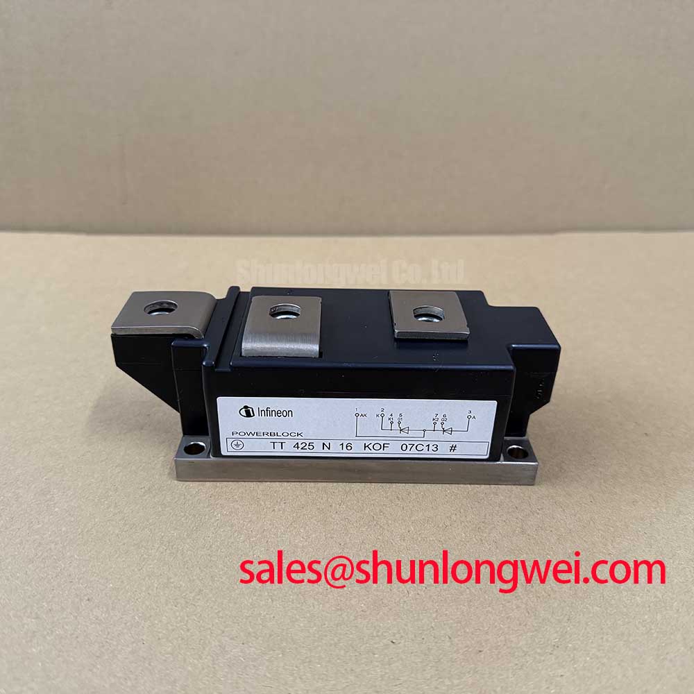
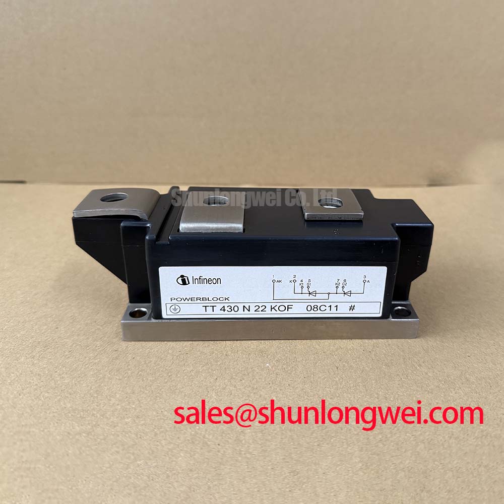
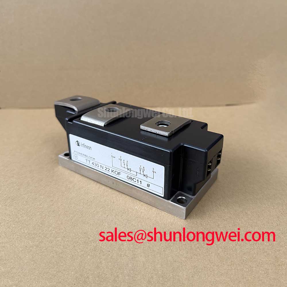
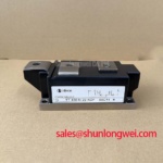
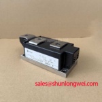
Before connecting the power circuit, isolate the assembly and compare the cold diode mode readings between each accessible main terminal path against a known good installation or the original circuit documentation. The TT430N22KOF is an Infineon dual thyristor module with a 2200 V repetitive peak off state and reverse voltage rating, stated as an Official Datasheet Specification. Its 430 A average on state current rating at Tc = 85°C is a rated current value under the specified case temperature and datasheet conditions; it should not be treated as a standalone continuous current limit for every rectifier assembly.
A semiconductor fuse must be coordinated from its own published clearing curve and total clearing energy, then compared with the thyristor protection limits stated in the applicable manufacturer documentation. The supplied official parameter set for this module identifies a 14500 A surge on state current rating for a 10 ms event at 25°C, but does not provide a module specific fuse coordination I²t value. It would therefore be incorrect to declare a particular fuse rating or fault clearing result for this model without the original fuse data, circuit prospective fault current, and manufacturer protection information.
| Official specification | Value | Integration relevance |
|---|---|---|
| Repetitive peak voltage | 2200 V | Verify against line transient and rectifier blocking conditions. |
| Average on state current | 430 A at Tc = 85°C | Assess against the measured cooling base temperature and load profile. |
| Surge on state current | 14500 A for 10 ms at 25°C | Use as a fault and inrush verification boundary, not as continuous capability. |
| Thermal resistance junction to case | 0.062 K/W per thyristor | Supports thermal path assessment for each thyristor section. |
| Maximum junction temperature | 125°C | Absolute thermal operating limit. |
Terminal hardware, conductor alignment, contact cleanliness, and mounting force should be checked against the original module documentation and equipment drawing. The supplied factory data does not define mounting torque, stud size, or terminal layout, so these details must not be inferred from the current rating. 💡 Bench Tip: Keep gate and main terminal leads disconnected until cold state reference readings have been recorded, because residual cabinet energy can invalidate the measurement and damage test equipment.
TT430N22KOF Operational Boundaries: Evaluating Sinusoidal 10 ms Half Cycle Surge Current Limits
The 14500 A, 10 ms, 25°C surge current figure is an Official Datasheet Specification for a defined short duration condition. It is not a permission to repeat high current events at arbitrary case temperatures or to assume unchanged capability after a preceding overload. For an incoming inspection record, note the measured heatsink temperature, the expected line half cycle waveform, protective device status, and whether reverse voltage is reapplied after the disturbance.
Thermal evaluation must also account for the stated 0.062 K/W junction to case thermal resistance per thyristor. This value describes the thermal path from each thyristor junction to the module case under the manufacturer’s specified conditions; it does not include interface material, heatsink spreading resistance, coolant performance, or cabinet airflow. Design Consideration: verify the complete thermal path with representative rectifier loading, because a case temperature that appears acceptable can still leave insufficient junction temperature margin during uneven phase loading or repeated overload recovery.
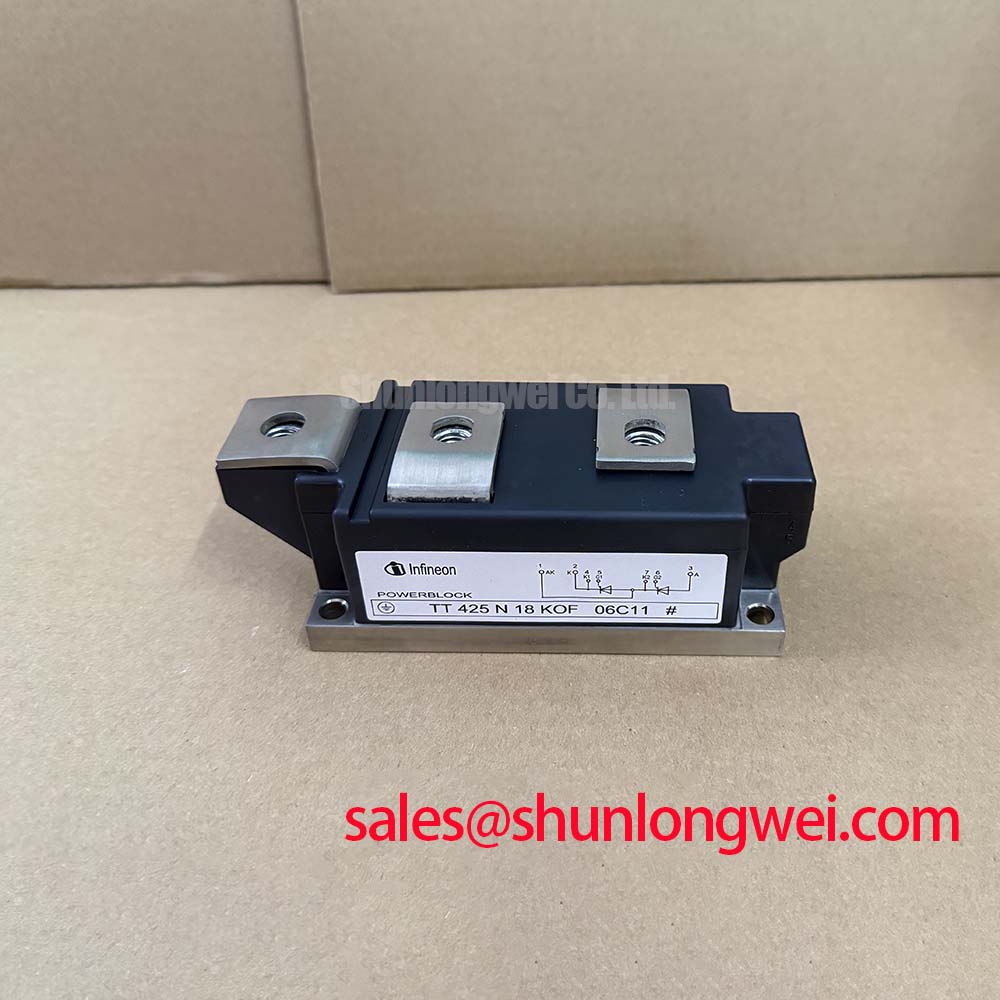
For high current green hydrogen electrolyzer DC power rectifiers, engineers can assess this module where voltage blocking, current waveform, cooling arrangement, and gate control match the original converter requirements. A TT500N18KOF can be reviewed as a separate device reference when documenting adjacent rectifier or auxiliary power stages, but its electrical ratings and mechanical interface must be verified independently. A TT570N16 is likewise a reference point for comparison only, rather than an automatic replacement decision.
Field Diagnostics and Commissioning: Power Factor Degradation and Harmonic Mitigation in TT430N22KOF Topologies
During commissioning, confirm the firing order at the isolated gate drive outputs before applying main power, then compare the phase current waveforms and DC output ripple with the known converter control sequence. In a controlled thyristor rectifier, moving the firing angle from near zero toward later conduction angles changes the DC transfer characteristic and generally increases reactive power demand. The exact relationship depends on rectifier topology, source impedance, commutation overlap, transformer arrangement, and load conditions.
If DC output becomes unstable, low power factor or harmonic symptoms should not be assigned to the module alone. Check firing pulse presence at every gate channel, phase voltage balance, cable continuity, snubber condition where fitted, control reference integrity, cooling performance, and current feedback calibration. A missing or delayed gate pulse may produce an asymmetric waveform, while commutation effects and supply distortion can produce similar observations. Engineering Recommendation: capture synchronized line voltage, phase current, gate command, and DC output signals before changing control timing.
The 2200 V repetitive blocking rating should be checked against the voltage actually applied across the device, including phase-to-phase and transient conditions in the equipment, rather than only the nominal AC line voltage. Design Consideration: minimize unintended conductor loop area where transient energy can create additional blocking stress, then verify peak conditions during controlled switching and fault recovery tests. For broader context on power semiconductor operating principles, see The Ultimate IGBT Knowledge Base.
TT430N22KOF Circuit Protection and Reliability: Calibrating High di/dt Gate Firing Pulse Train Timing
The available factory information identifies voltage, current, surge, thermal resistance, and maximum junction temperature limits, but does not specify gate trigger current, gate trigger voltage, permissible gate current rise rate, holding current, latching current, or pulse train duration. Those gate drive parameters must be verified from the original manufacturer documentation for the exact module and from the installed converter design. They should not be reconstructed from a generic dual thyristor module profile.
Where the control system uses repeated gate pulses, inspect pulse polarity, timing symmetry, isolation performance, return path continuity, and alignment with the intended anode to cathode voltage condition. A gate signal can be present at a connector yet still fail to produce reliable turn on if the reference path, pulse energy, or phase timing is compromised. Conversely, a sustained abnormal gate drive condition requires investigation of the driver circuit and its protective elements before a replacement module is energized.
Industry resources on module interconnection and package level reliability can inform a general Design Consideration, but they are not product specific evidence for the TT430N22KOF. Infineon’s .XT Technology article discusses power semiconductor interconnection concepts, while the CIPOS™ Nano IPM Series illustrates a different integrated power module category. Neither source should be used to assign unlisted gate drive or reliability ratings to this dual thyristor module.