Content last revised on July 5, 2026
Fuji Electric 6DI15MS-050: A Technical Review of the 6-in-1 Darlington Power Transistor Module
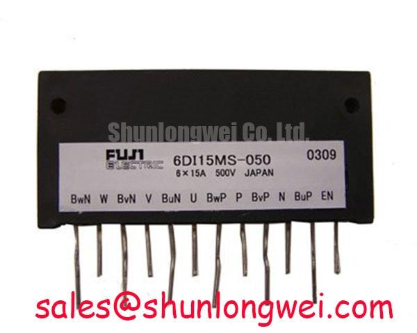
The Fuji Electric 6DI15MS-050 is a Darlington Transistor Module engineered for robust performance in low to medium frequency power control applications. This device integrates six Darlington transistor circuits with free-wheeling diodes into a single, compact package, offering a streamlined solution for three-phase inverter circuits. Key specifications include a **Collector-Emitter Voltage (VCEO) of 450V** and a continuous **Collector Current (IC) of 15A**. The module's primary engineering benefit is its high DC current gain (hFE), which significantly simplifies the required base drive circuitry, a critical factor in the design and maintenance of legacy industrial equipment. For systems requiring straightforward, reliable power switching without the complexity of modern high-frequency IGBT gate drives, the 6DI15MS-050 provides a proven and effective solution. Its design is best suited for applications like small motor drives and power supplies where durability and ease of implementation are paramount.
Key Parameter Overview
Decoding the Specs for System Reliability
The technical specifications of the 6DI15MS-050 are tailored for durability and stable performance in demanding industrial environments. Understanding these parameters is key to leveraging the module's full potential in power circuit design.
| Parameter | Value | Significance |
|---|---|---|
| Collector-Emitter Voltage (VCEO) | 450V | Provides a sufficient safety margin for applications operating on 200/230V lines. |
| Collector-Base Voltage (VCBO) | 600V | Indicates the maximum voltage the collector-base junction can withstand, critical for handling voltage transients. |
| Continuous Collector Current (IC) | 15A | Defines the maximum steady-state current the device can handle, suitable for small horsepower motor drives. |
| Peak Collector Current (ICP) | 30A | Specifies the module's ability to handle short-duration current surges, essential for motor startup conditions. |
| DC Current Gain (hFE) | 75 (Min) at IC=15A | A high gain simplifies the base drive circuit, reducing component count and power requirements for the control stage. |
| Collector-Emitter Saturation Voltage (VCE(sat)) | 2.5V (Max) | This parameter is crucial for calculating conduction losses. A lower VCE(sat) means less power is dissipated as heat, improving overall efficiency. Think of it as the 'voltage cost' of turning the switch on; the lower the cost, the cooler the operation. |
| Total Power Dissipation (Pc) | 125W | Dictates the maximum amount of heat the module can dissipate, a fundamental value for proper Thermal Management and heatsink selection. |
Application Scenarios & Value
System-Level Benefits in Industrial Motor Control
The 6DI15MS-050 is optimized for power conversion systems where switching frequencies are typically below 20 kHz. Its primary value lies in providing a robust, all-in-one solution for legacy and new designs focusing on reliability over cutting-edge speed. For engineers working on small-scale industrial automation, this module presents a practical and efficient component.
A high-fidelity engineering scenario for this module is in the refurbishment or design of a simple Variable Frequency Drive (VFD) for a 3-phase AC motor up to approximately 2.2 kW. In such a system, a key challenge is designing a base drive circuit that is both reliable and cost-effective. The high hFE of the 6DI15MS-050 directly addresses this challenge. Unlike single BJT transistors that require significant base current, this Darlington module needs only a fraction of that current to achieve full saturation. This allows for the use of smaller, less powerful, and less complex driver components, reducing both the bill of materials (BOM) and the potential points of failure within the control stage. The integrated free-wheeling diodes further simplify the design by providing a built-in path for inductive motor currents, eliminating the need for six external high-current diodes and simplifying the PCB layout. While modern designs might use an IPM, for cost-sensitive or legacy system repairs, the 6DI15MS-050 offers an excellent balance of performance and design simplicity.
For applications demanding higher current capabilities, the related 6DI100A-060 provides a collector current of 100A within a similar technology class.
Frequently Asked Questions (FAQ)
Engineering Insights for the 6DI15MS-050
What is the primary advantage of the 6DI15MS-050's Darlington configuration compared to a modern IGBT?
The main advantage is its high DC current gain (hFE). This simplifies the base drive circuitry, requiring significantly less current from the control board to switch the main load. This is particularly beneficial in older or simpler VFD and Servo Drive designs where complex gate driver ICs may not be used.
How does the VCE(sat) of 2.5V impact thermal design?
The VCE(sat) of 2.5V directly contributes to conduction losses (Power Loss = VCE(sat) x IC). A higher VCE(sat) compared to modern IGBTs means more heat is generated during operation. Therefore, effective heatsinking and thermal management are critical. Engineers must use this value to accurately calculate thermal resistance requirements for the heatsink to keep the junction temperature within its Safe Operating Area (SOA).
Is the 6DI15MS-050 suitable for high-frequency applications like switching power supplies?
No, this module is not ideal for high-frequency switching. Darlington transistors have inherently slower turn-on and turn-off times compared to IGBTs or MOSFETs. Using it at high frequencies would result in excessive switching losses, leading to inefficiency and potential thermal failure. It is best suited for applications below 20 kHz, such as motor control and welding power supplies.
What is the function of the integrated free-wheeling diodes?
The free-wheeling diodes (FWDs) are essential in circuits that drive inductive loads like motors. When a transistor turns off, the energy stored in the motor's inductance creates a voltage spike. The FWD provides a safe path for this current to circulate, protecting the transistor from reverse voltage damage. Integrating them into the module saves space and simplifies the overall circuit design.
For design engineers and procurement specialists focused on maintaining the operational integrity of established industrial systems, the 6DI15MS-050 offers a targeted solution. Its value proposition is not in competing with the latest semiconductor technology, but in providing a reliable, easily integrated power stage for low-frequency, three-phase applications. By simplifying drive requirements and integrating key components, it serves as a strategic choice for extending the lifecycle of valuable industrial machinery and for new designs where robustness is the foremost priority.