
Content last revised on September 10, 2026
Galvanic Gate Drive Isolation, Reinforced Creepage & High-CMTI Signaling
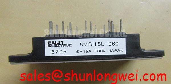
In high-precision motion control architectures, such as precision stepper systems and brushless DC (BLDC) servo actuators, the gate drive interface represents the primary defensive boundary between sensitive digital logic and the high-voltage inverter stage. The 6MBI15L-060 from Fuji Electric is engineered as a compact 6-pack (six-pack) topology rated at a collector-emitter voltage of VCES = 600V (Official Datasheet Specification) and a continuous collector current of IC = 15A (Official Datasheet Specification). When deploying this module into a 200V to 240V AC rectified bus environment (generating nominal DC link voltages between 280V and 340V DC), rapid switching transients generated by pulse-width modulation (PWM) introduce severe common-mode noise across the isolation barrier.
Field diagnosis of premature driver failure or erratic motor stepping frequently points to inadequate Common-Mode Transient Immunity (CMTI) in the gate drive optocouplers or digital isolators. During hard switching events, high-speed dV/dt transients exceeding 15 kV/µs can couple through the parasitic capacitance of the isolation barrier, injecting displacement current directly into the gate driver's secondary output stage. This parasitic injection often induces spurious gate turn-on pulses, causing shoot-through events across the upper and lower arms of the three-phase bridge. For robust field operation, gate drive circuitry serving the 6MBI15L-060 must utilize isolation ICs with a minimum CMTI rating of 100 kV/µs, combined with reinforced galvanic isolation rated to withstand dielectric test voltages above 2.5 kV RMS for 60 seconds.
High-voltage insulation integrity also demands rigorous adherence to PCB creepage and clearance distances surrounding the solder pins. Industrial environments subject servo drives to particulate contamination, humidity, and conductive dust over extended operating cycles. When laying out the printed circuit board for the 6MBI15L-060, engineers should maintain a minimum physical clearance of 3.2 mm and a creepage distance of at least 6.3 mm along the high-voltage traces (Design Consideration under IEC 60664-1 Pollution Degree 2, Material Group IIIa). If tight chassis constraints prevent these spacing dimensions, milling physical isolation slots (air gaps) directly between the high-voltage collector pins and low-voltage signal traces prevents surface tracking and breakdown.
To evaluate legacy gate drive designs or cross-reference gate performance against modern discrete alternatives, field engineers can examine technical topologies detailed in Fuji Electric High-Speed Discrete IGBTs. On the service bench, when troubleshooting unexplained overcurrent trips on a malfunctioning axis, verify the gate-to-emitter bias voltage with a high-bandwidth isolated differential oscilloscope probe. Ensure the positive gate bias delivers a stable +15V ± 10% (Design Consideration for full channel saturation), while a dedicated negative turn-off bias of -5V to -8V is applied to clamp the gate against capacitive Miller feedback currents during complementary arm commutations.
Turn-Off di/dt Induced V_peak Clamping and Snubber Capacitor Sizing
During turn-off commutation under full load, the rapid interruption of the 15A collector current generates substantial di/dt across the parasitic stray inductances distributed throughout the power loop. The instantaneous peak collector-emitter voltage is governed by the relation where the peak terminal voltage equals the DC bus voltage augmented by the product of the total loop parasitic inductance and the turn-off di/dt rate. With the 6MBI15L-060 rated at a maximum VCES of 600V, an unregulated DC link running at 380V combined with a high turn-off di/dt of 300 A/µs and a modest loop inductance of 80 nH will easily generate transient spikes exceeding 404V, rapidly eroding the silicon safety margin.
Minimizing this transient overvoltage demands both physical busbar optimization and localized capacitive snubbing. Symmetrical planar laminated DC busbars should be used to overlap the positive (P) and negative (N) conductors, utilizing mutual magnetic flux cancellation to compress the total parasitic loop inductance below 25 nH. To suppress residual high-frequency ringings directly at the module terminals, high-frequency polypropylene film snubber capacitors (typically sized between 0.1 µF and 0.47 µF with low Equivalent Series Inductance, rated for 630V DC or higher) must be mounted in immediate proximity to the primary DC input pins of the module.
| Physical / Electrical Parameter | Official Specification / Engineering Value | Field Application Context & Impact |
|---|---|---|
| Collector-Emitter Voltage (VCES) | 600V (Official Datasheet Specification) | Provides steady operating margin for 200–240V AC rectified motion drives. |
| Continuous Collector Current (IC) | 15A at TC = 25°C (Official Datasheet Specification) | Suited for fractional-horsepower BLDC and micro-stepping actuator bridges. |
| Maximum Power Dissipation (Pc) | 60W per element (Official Datasheet Specification) | Demands precise thermal interface material application and heatsink sizing. |
| Internal Topology | 6-Pack / Three-Phase Inverter Bridge | Integrates 6 IGBTs with antiparallel fast-recovery freewheeling diodes. |
| Mounting Hardware Torque | 2.5 to 3.5 N·m (Design Consideration for M5 Screws) | Ensures uniform mechanical baseline without fracturing the internal ceramic substrate. |
When scaling industrial motion platforms or reviewing legacy hardware across various machine generations, engineers encountering larger multi-axis cabinets may compare this compact 6-pack to higher-capacity configurations; for systems demanding higher current handling in specialized braking or multi-module layouts, the related 2MBI300J-060 provides a dual-pack configuration rated for up to 300A at 600V. Regardless of scale, proper thermal transfer must be maintained across the baseplate.
⚠️ Field Alert: During field replacements of the 6MBI15L-060, always remove all oxidized compound from the heatsink mating surface using an industrial solvent. Apply a uniform layer of high-thermal-conductivity silicone grease (thermal conductivity ≥ 1.5 W/m·K) strictly between 50 µm and 100 µm in thickness. Excessive grease application creates a thermal barrier that causes localized junction overheating, while uneven screw tightening risks cracking the internal Direct Bonded Copper (DBC) ceramic substrate. Tighten mounting screws in a progressive two-stage cross-pattern, finishing at a verified torque of 2.5 to 3.5 N·m (General Industry Design Consideration for standard M5 hardware).
SCSOA Overcurrent Protection: Implementing Two-Step Gate Voltage Clamping
Short-circuit withstand capability is a decisive operational factor in servo motor actuators, where mechanical jams, phase-to-phase shorts, or earth faults inside motor windings subject the power stage to destructive current surges. Under the Short-Circuit Safe Operating Area (SCSOA) boundaries, the 6MBI15L-060 is designed to withstand short-circuit conditions for a maximum duration of tsc ≤ 10 µs (Design Consideration under VCC = 400V, VGE = 15V, Tj ≤ 125°C). If the fault current is not fully extinguished within this 10 µs window, thermal runaway from localized current filamentation will cause catastrophic silicon rupture.
Standard desaturation (DESAT) detection schemes continuously monitor the forward collector-emitter voltage across the active switch. Under nominal operating conditions, the on-state saturation voltage remains low: VCE(sat) ≈ 1.95V to 2.4V at rated IC (Typical Starting Point for benchmarking). When a hard short circuit (Type I fault) or a load fault during conduction (Type II fault) occurs, the collector current spikes to 4 to 6 times the rated current, dragging the IGBT out of saturation and causing VCE to climb rapidly toward the full DC link voltage. A high-voltage blocking diode connected to the DESAT pin senses this rise; once VCE crosses an established reference threshold (typically set between 6.5V and 8.0V), the driver initiates an emergency shutdown sequence.
Direct, abrupt gate shutdown during a severe short-circuit fault generates an extreme di/dt that inevitably triggers fatal overvoltage spikes across the module terminals. To preserve the device, gate drive topologies must incorporate Two-Step Gate Voltage Clamping (Soft Turn-Off). Upon desaturation detection, the driver first clamps the gate-emitter voltage down from +15V to an intermediate level of approximately +8V to +10V for a period of 1.5 µs to 2.5 µs. This step drastically reduces the instantaneous channel conduction current and curtails the subsequent di/dt. After this brief decay window, the driver pulls the gate fully down to its negative bias level. For comprehensive bench-testing methodology, oscillographic waveform verification, and root-cause inspection protocols, technicians can reference the testing and diagnostic frameworks compiled in the Field Engineer’s Handbook.
PCB Symmetry Considerations for Dual IGBT Half-Bridge Switching Paths
In high-dynamic servo positioning systems, asymmetrical PCB layout paths across the three inverter phases produce unequal stray inductances, leading to current imbalance, phase jitter, and differential electromagnetic radiation. The compact footprint of the 6MBI15L-060 combines all six switches within a single housing, which makes PCB trace routing around the terminal pins a critical engineering consideration. The primary source of parasitic gate-drive oscillation is magnetic and capacitive coupling between the high-current power emitter loops and the low-current gate return paths.
To eliminate unwanted inductive feedback, the PCB layout must strictly isolate the power emitter return traces from the auxiliary Kelvin emitter gate connections. When the load current undergoes rapid di/dt, any stray inductance shared between the gate driver loop and the main collector-emitter power loop induces an opposing voltage into the gate drive loop (LE · di/dt). This voltage directly subtracts from the applied gate bias, inducing severe gate ringing, unintended turn-off delays, or high-frequency parasitic oscillations that degrade switching efficiency and elevate EMI emissions.
- Kelvin Return Separation: Route the auxiliary emitter signal directly from the module pin to the gate driver IC ground using a dedicated, narrow PCB trace, preventing any power stage load current from flowing through the signal return path.
- Minimization of Gate Loop Area: Position the forward gate trace and the auxiliary emitter return trace on adjacent PCB layers directly overlapping one another, or run them as closely coupled parallel pairs to minimize the physical magnetic pickup loop area.
- Gate Damping Resistance: Locate the series turn-on and turn-off gate resistors (with a calculated starting value of RG = 15 Ω to 33 Ω (Typical Starting Point for bench tuning)) within 10 mm of the module's physical pins to dampen resonant LC tank circuits formed by the internal gate capacitance and trace inductance.
- Reflected Wave Mitigation: In industrial setups where long motor cables connect the inverter to the actuator, the rapid dV/dt (often > 5 kV/µs) interacts with the transmission line characteristics of the cable, producing reflected wave overshoots that can double the peak voltage at the motor terminals. Symmetrical dV/dt output chokes or RC snubber filters should be integrated at the drive output terminals to restrict edge rates below 1 kV/µs.
When engineering auxiliary power systems, dynamic braking units, or high-current feeding stages within the same multi-axis motion control cabinet, engineers often implement discrete dual-pack topologies; in such system-level power allocations, the complementary 2MBI150-060 serves as a dual-IGBT half-bridge building block rated at 150A and 600V. Maintaining layout symmetry across all output phases—whether using all-in-one six-packs like the 6MBI15L-060 or discrete half-bridge configurations—ensures uniform thermal distribution across the heatsink, prevents localized gate jitter, and guarantees clean dynamic commutation under continuous heavy-duty industrial cycling.