Content last revised on September 10, 2026
Assembly Integrity & Layout Architecture: Implementing High-Speed Fault Management with VCE Desaturation for 1DI300ZN-120-02
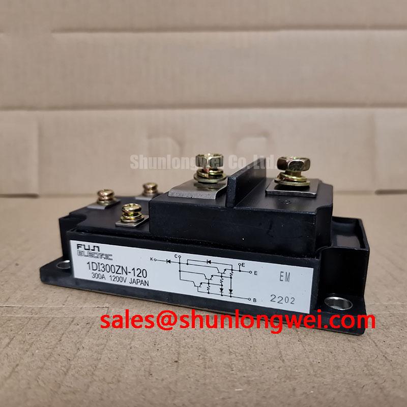
With the drive fully isolated and the DC link discharged, first inspect the 1DI300ZN-120-02 terminal area, power connections, mounting surface, and module housing for loose hardware, overheating marks, cracked insulation, or contamination before any replacement decision is made. This Fuji Electric power transistor module is officially rated at 1200 V and 300 A, with a Power Transistor Module package classification. These specifications should be matched against the original drive bill of materials and electrical limits.
| Parameter | Official Specification |
|---|---|
| Manufacturer | Fuji Electric |
| Module model | 1DI300ZN-120-02 |
| Rated voltage | 1200 V |
| Rated current | 300 A |
| Package category | Power Transistor Module |
Before energizing a repaired heavy-duty variable-frequency AC motor drive, verify that the gate driver connection, collector path, emitter return path, and DC bus terminals correspond exactly with the original circuit layout. A cold resistance check can identify an obvious low-impedance power path, but it cannot prove switching integrity. Compare measurements with a known-good phase position where available, then inspect the driver board for damaged isolation components, gate resistors, and desaturation sensing parts.
Desaturation monitoring is a design consideration for an inverter using this class of 1200 V, 300 A power module. The protection circuit observes collector-to-emitter behavior while the switch is commanded on, allowing the control system to respond when the switching state no longer matches expected load conditions. Type I and Type II short-circuit behavior must be assessed against the module documentation and the actual inverter topology. Protection response timing, blanking behavior, and threshold selection are system-determined and require switching verification on the completed equipment.
A controlled two-stage soft turn-off sequence is commonly evaluated where abrupt interruption of fault current could create damaging inductive overshoot. Keep the gate driver return path compact and separate its sensing reference from noisy power-current paths where the original layout permits. ⚠️ Field Alert: Do not reconnect gate or power wiring until the DC link has been confirmed discharged and the original terminal orientation has been verified.
Fuji Electric’s power semiconductor and IPM module information provides useful manufacturer context when checking module family compatibility, while the final protection implementation must remain tied to the equipment schematic and approved service procedure.
1DI300ZN-120-02 Circuit Protection & Reliability: Calibrating Regenerative DC Bus Voltage Surge Dissipation
During motor deceleration, a variable-frequency drive can return mechanical energy to the DC bus. The braking path, braking transistor arrangement, and ballast resistor must therefore be examined as a complete energy-handling system rather than as isolated parts around the 1DI300ZN-120-02. A bus overvoltage event may involve load inertia, incorrect drive programming, an open braking resistor connection, a failed braking control circuit, or an unsuitable regeneration path. Measure and compare the DC bus waveform with the equipment’s approved reference limits before assigning a root cause.
Minimizing busbar loop inductance is an engineering recommendation when suppressing switching overshoot. The DC-link film capacitor should remain physically and electrically close to the inverter commutation loop where the original mechanical design supports it. MOV-based surge suppression can also be evaluated as part of the surrounding protection network, but its clamping behavior, energy capability, and coordination with fuses and contactors must be validated by the system engineer.
For repair assessment, inspect capacitor terminals, busbar joints, braking resistor wiring, and insulation clearances for heat damage or mechanical movement. Creepage and clearance requirements are determined by the complete drive’s working voltage, pollution environment, enclosure construction, and applicable safety standard. Do not infer independent EMC, insulation, or safety certification from the module itself.
Where a circuit comparison is required, the 6MBI300U-120 can be reviewed as a separate Fuji Electric module reference. Its topology, terminal arrangement, gate-drive requirements, thermal interface, and control behavior must be checked against the original design before any compatibility decision.
Assembly Integrity & Layout Architecture: Implementing Thermal Time Constants and Peak Junction Temperature for 1DI300ZN-120-02
Thermal diagnosis starts at the interface between the module base and heatsink. Remove old interface material carefully, inspect both contact surfaces for flatness and debris, and confirm that mounting hardware is tightened in the documented sequence for the installed equipment. A thin, uniform thermal compound layer is a design consideration intended to reduce interface voids; the required material and fastening method are determined by the drive manufacturer’s assembly instructions.
Peak junction temperature during overload cannot be calculated from the 300 A nameplate current alone. It depends on switching losses, conduction losses, pulse duration, coolant or fan performance, heatsink condition, ambient temperature, and the transient thermal impedance data applicable to the module. An engineering calculation using a validated multi-RC thermal model can estimate the junction response, but only when manufacturer thermal data and measured operating conditions are available.
Inspect cooling fans, airflow channels, heatsink fins, and temperature-sensing connections before declaring a power module fault. Repeated thermal trips may indicate restricted airflow, a loose temperature sensor, changed load duty, or control calibration issues. The official information supplied for this module does not state surge-current or lifetime figures, so no such values should be assumed during service planning.
Transient Dynamics & Electrical Design: Suppressing Cres-Induced Gate Voltage Spikes on 1DI300ZN-120-02
Unexpected gate-voltage movement during rapid collector-voltage transitions can contribute to cross-conduction in an inverter leg. Inspect the gate-driver board for equal return routing, degraded gate resistors, damaged isolated-driver outputs, and poor connector contact. An oscilloscope measurement referenced with appropriate isolated probing can help determine whether the observed event follows the intended gate command or is coupled from the power-switching node.
An active Miller clamp and negative gate bias are design considerations often assessed in high-noise gate-drive systems, particularly where rapid voltage transitions can disturb an off-state device. The necessary bias level, clamp arrangement, isolation capability, and common-mode transient immunity are determined by the driver architecture and must be validated against measured gate voltage and DC bus transients. Avoid extending gate leads or sharing a gate return with high-current power paths, as both conditions can worsen noise coupling.
For broader reading on fast-switching behavior in three-phase conversion, review The 1200 V CoolSiC™ MOSFET Advantage in Three. It is useful as a general switching design reference, while the 1DI300ZN-120-02 must be integrated according to its own official ratings, original drive circuit, and verified commissioning results.