Content last revised on September 10, 2026
1DI300A-140 Circuit Protection & Reliability: Calibrating Baseplate Convexity Compensation and Screw
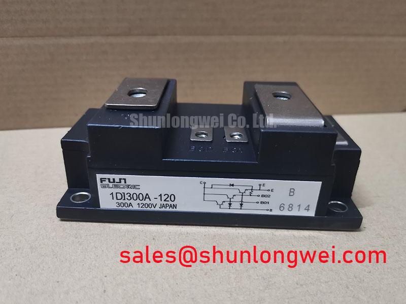
Before fitting the 1DI300A-140, isolate the equipment, inspect the baseplate and heatsink contact faces for debris or distortion, and verify that the inverter DC bus remains within the system’s validated switching boundary. This Fuji Electric power transistor module is officially rated at 1400 V collector emitter voltage and 300 A continuous collector current at TC = 80°C. Its typical collector emitter saturation voltage is 2.7 V at 300 A, a value relevant to conduction loss estimation and heatsink assessment in high current power stages.
The module can be evaluated for industrial inverter welders and medium frequency induction heating power supplies where the existing circuit topology, gate drive arrangement, cooling hardware, and protection thresholds have been checked against the original equipment documentation. The official square reverse bias safe operating area extends to 1400 V, supporting assessment of demanding inductive turn off conditions. The official short circuit withstand time is 10 μs at VCC = 900 V and VGE = 15 V; protection hardware must therefore detect and control abnormal current within the capability of the complete system.
A flat, clean thermal stack is the starting point for reliable service. Baseplate flatness, heatsink condition, and mounting hardware all influence the thermal path from the module into the cooling assembly. As a general installation practice, maintenance teams can apply thermal interface material as a controlled, continuous layer and inspect the contact pattern after an initial fit. A thermal interface thickness in the 50 to 100 μm range is a Design Consideration, not an official module specification; the suitable thickness depends on the interface material, baseplate condition, and heatsink surface quality.
Where baseplate curvature or heatsink unevenness is suspected, do not attempt to correct it by concentrating pressure at one mounting point. Bring screws down progressively in a cross pattern so the assembly settles evenly. The applicable torque must be taken from the module mechanical documentation and the equipment manufacturer’s fastening specification. Uneven clamping can create local interface voids, which may appear later as abnormal temperature rise during heavy duty operation.
⚠️ Maintenance Note: During planned service, monitor terminal and heatsink contact temperature rise under representative load, then clear blocked airflow paths and recheck mounting tightness after the equipment has cooled.
For a hardware substitution review, the 6MBI300U-120 should be treated as a separate module requiring independent verification of circuit function, terminal arrangement, gate drive requirements, mechanical fit, and protection coordination rather than as an automatic replacement.
Field Diagnostics & Commissioning: Thermal Time Constants and Peak Junction in 1DI300A-140 Topologies
Commissioning after a repair should begin with controlled low energy operation, followed by measurement of current, DC bus behavior, gate waveforms, and thermal response as load is increased. The 2.7 V typical VCE(sat) at IC = 300 A is an Official Datasheet Specification and provides a useful reference for calculating conduction dissipation, but it is not a fixed field measurement limit. Device temperature, gate drive conditions, load waveform, and measurement arrangement can all affect observed voltage.
During pulsed overload analysis, the junction temperature does not immediately equal the case temperature. A multi RC transient thermal model, when available from the relevant manufacturer data, allows the system engineer to combine pulse power and pulse duration with the transient junction to case response. This is an Engineering Calculation requiring the actual thermal model, measured duty cycle, cooling condition, and verified starting temperature. It should not be replaced with a single assumed thermal resistance.
For maintenance work, a thin and uniform thermal interface layer is usually preferable to an excessively thick layer that increases thermal path resistance. A 50 to 80 μm target may be used as a general Design Consideration where the selected interface material and mounting surfaces support it. Check the equipment’s fan performance, liquid cooling flow where applicable, filter cleanliness, and evidence of condensation before judging the module from temperature behavior alone.
In power systems incorporating a rectifier or related front end stage, the 6MBP100TEA060-50 is a related topology component that should be checked separately for its own voltage, current, cooling, and connection requirements.
1DI300A-140 Operational Boundaries: Evaluating Desaturation Detection Limits
The official 10 μs short circuit withstand time at VCC = 900 V and VGE = 15 V defines a critical survival interval under the stated test condition. It does not establish a universal protection delay for every inverter. Desaturation detection, current sensing, blanking behavior, gate driver response, and turn off dynamics must be validated together on the finished power assembly.
A practical diagnostic sequence is to review whether the gate driver responds consistently during commanded switching, then capture collector emitter voltage and current with measurement methods suitable for the voltage and energy present. An unexpected desaturation response may indicate a gate drive issue, load fault, wiring problem, current sensor concern, or switching loop condition. Compare measurements with a known healthy channel or the original circuit documentation before replacing parts.
Soft turn off can be considered as a Design Consideration where fault interruption creates inductive voltage overshoot. The objective is to control the current fall rate while ensuring the switching event remains inside validated electrical limits. Minimize parasitic inductance in the gate and power loops to suppress turn off overshoot, then verify peak collector emitter voltage against the DC link and the module’s 1400 V VCES rating during controlled switching tests. Practical gate drive test methods are discussed in Precision Gate Drive Design.
For broader context on high power semiconductor module integration and device families, consult Powerex High Power Semiconductor Modules.
Field Diagnostics & Commissioning: Cosmic Ray Robustness: Voltage Derating Cu in 1DI300A-140 Topologies
No quantified cosmic ray, neutron induced failure rate, altitude derating curve, or single event burnout qualification is stated in the supplied official parameters for the 1DI300A-140. It would therefore be inappropriate to assign a FIT value, predicted operating life, elevation limit, or mandatory DC bus derating percentage to this module.
For installations at elevated sites or in equipment exposed to unusual environmental conditions, altitude and environmental margin are Design Considerations for the entire converter, not a device only judgment. The system integrator should review enclosure cooling capacity, humidity control, contamination level, insulation coordination, DC bus transient records, and protection behavior using the original system safety requirements. This approach is particularly important where an industrial inverter welder or induction heating supply has been relocated, modified, or returned to service after a prolonged shutdown.
Commissioning records should retain measured DC bus voltage, switching waveform captures, cooling condition, load profile, and protection trip observations. These objective records help distinguish a transient system event from a thermal interface issue, gate drive inconsistency, external load fault, or degraded cooling path without assigning unsupported failure mechanisms to the module.