Content last revised on September 3, 2026
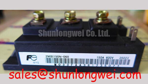
Fuji Electric 2MBI150J-060 Inspection and Ratings
With the power stage isolated and discharged, begin incoming inspection of the Fuji Electric 2MBI150J-060 by comparing the terminal map on the module case with the original equipment documentation, then use a multimeter diode function to check each intended freewheel-diode path before applying gate drive.
This is a dual IGBT module rated at VCES = 600 V and IC = 150 A at TC = 80°C under the official datasheet conditions. Its specified pulsed collector current is 300 A for 1 ms, while the continuous gate emitter voltage limit is ±20 V. These ratings define the device identity and should be checked against the original inverter topology, DC link voltage, cooling arrangement, gate driver behaviour, and control-board interlocks before replacement evaluation.
| Official datasheet parameter | Test condition | Specification |
|---|---|---|
| Collector emitter voltage, VCES | Tvj = 25°C | 600 V |
| Continuous collector current, IC | TC = 80°C | 150 A |
| Pulsed collector current, ICP | tp = 1 ms | 300 A |
| Gate emitter voltage, VGES | Continuous | ±20 V |
| Power dissipation per device, PC | TC = 25°C | 600 W |
| Collector emitter saturation voltage, VCE(sat) | IC = 150 A, VGE = 15 V | 2.2 V typical, 2.8 V maximum |
| Gate emitter threshold voltage, VGE(th) | IC = 150 mA, VCE = 20 V | 5.0 V to 8.0 V |
| Diode forward voltage, VF | IF = 150 A, VGE = 0 V | 2.2 V typical, 2.8 V maximum |
| IGBT junction to case thermal resistance, Rth(j c) | Per IGBT device | 0.21°C/W |
| Diode junction to case thermal resistance, Rth(j c) | Per FWD device | 0.36°C/W |
Preventing Spurious Faults: Thermal Feedback Guidelines for 2MBI150J-060
Before commissioning a repaired inverter welder or medium frequency induction heating supply, verify that each IGBT section has the expected cold state relationship between its main terminals and that the gate circuit is isolated from the power path. A diode mode test can identify an unexpected near short or an open diode path, but it does not establish switching health. Compare readings with a known good module only when the same meter, probe polarity, ambient condition, and terminal reference are used. The module must be disconnected from driver circuitry and surrounding parallel paths for this check to be meaningful.
The official 2.2 V typical and 2.8 V maximum VCE(sat) specification applies at 150 A with VGE = 15 V. In static parallel operating conditions, the positive temperature tendency of IGBT saturation voltage can assist current sharing after temperatures stabilize. That characteristic is not a substitute for matched drive paths. Dynamic current distribution remains sensitive to gate loop resistance, individual gate-driver propagation delay, common emitter impedance, busbar geometry, and the thermal condition of each mounting location.
💡 Bench Tip: Record cold diode mode readings and gate related resistance checks before energising the replacement assembly, then compare them again only after the equipment has fully discharged.
Design Consideration: where two devices are intended to share current, route their gate drive and return conductors with comparable physical paths and avoid allowing a high current emitter return to become part of one gate sensing loop. A drive path that appears electrically similar at low frequency can behave differently during a switching edge. Uneven turn on or turn off traces may indicate unequal loop coupling, driver asymmetry, gate network variation, or an issue elsewhere in the commutation circuit. Oscilloscope measurements should be taken against a known good signal path and with a probing method appropriate for high common mode switching conditions.
The module’s thermal values also require separate treatment for IGBT and freewheel diode losses. The IGBT junction to case value is officially specified as 0.21°C/W per IGBT device, while the diode junction to case value is 0.36°C/W per FWD device. A heatsink surface that seems uniformly warm does not prove equal junction stress, because conduction intervals and switching losses are controlled by the topology and load waveform. Verify mounting flatness, thermal interface coverage, clamping consistency, airflow, coolant performance where applicable, and the actual duty cycle imposed by the equipment.
For a higher voltage reference during compatibility review, the 2MBI200UB-120 is a separate Fuji Electric module with different electrical ratings and installation implications. It should be evaluated from its own official documentation rather than treated as a direct replacement for the 600 V 2MBI150J-060.
Field Diagnostics & Commissioning: SCSOA Overcurrent Protection in 2MBI150J-060 Topologies
Commissioning should begin with confirmation that the protection system can inhibit both complementary gate commands before full DC link energy is applied. In a bridge leg, simultaneous conduction is not diagnosed solely from a damaged module. It can arise from control logic, isolated driver supply behaviour, an interlock fault, timing corruption, connector issues, or gate loop disturbance. Check the controller’s command outputs, each driver output, the gate emitter waveform at the module reference point, and the DC link response in a controlled test sequence.
Short circuit protection must be designed around the actual short circuit safe operating area information and driver response of the installed system. No short circuit withstand duration is stated in the supplied official parameters for this product page. Therefore, a statement that the 2MBI150J-060 is protected by a particular detection interval would not be an official product specification. Engineering Recommendation: validate the total delay from fault onset through detection, logic processing, gate discharge, and IGBT current decay using the installed driver, layout, DC link, and operating temperature.
Desaturation monitoring is commonly used to observe a collector emitter voltage rise while the IGBT is commanded on. It must be coordinated with intentional turn on transients so that normal switching behaviour is not misread as a fault. Type I and Type II fault classifications used by a particular driver architecture should be confirmed from that driver’s documentation. When an overcurrent event is detected, a controlled soft turn off approach can reduce the abrupt current interruption that otherwise contributes to inductive overvoltage. The acceptable gate discharge profile is system determined and requires waveform verification against the voltage capability of the module and the transient capability of the surrounding circuit.
The ±20 V continuous VGES limit is an official device boundary, not a recommended operating drive voltage. The specified 5.0 V to 8.0 V VGE(th) is measured at only 150 mA collector current and should not be used as an on state drive target for a high current converter. Gate drive voltage, gate resistance, negative bias strategy if used, and dead time are all system level decisions that must be validated using the original driver requirements and measured switching results.
Design Consideration: dead time needs to prevent overlap despite differences in command timing, driver delay, switching temperature, and device turn off behaviour. Excessive dead time can alter output waveform quality and diode conduction, while insufficient dead time can permit shoot through. Inspect complementary interlock routing and confirm that an inhibit command reaches both gate drivers under each protection condition. The physical mechanism behind gate drain coupling during a voltage transition is described in the external reference on the Miller Effect and Gate to Drain Capacitance; the module specific switching limits must still be taken from applicable manufacturer data.
2MBI150J-060 Circuit Protection & Reliability: Calibrating Junction to Case Thermal Network Simulation
A thermal simulation for the 2MBI150J-060 should keep the IGBT and freewheel diode paths distinct. The official steady state junction to case thermal resistance values provide useful boundary data, but they do not by themselves describe transient thermal impedance during an overload pulse. A multi RC thermal network can be used when the necessary transient thermal data is available from authoritative product documentation. The simulation should then be correlated with measured case temperature, actual load waveform, cooling conditions, and switching behaviour rather than treated as an independent proof of junction temperature.
For a heavy pulse, estimated junction rise is governed by the energy dissipated in the relevant IGBT or diode interval and the time dependent thermal impedance from junction to case. The correct calculation depends on actual current, collector emitter voltage during switching, conduction duration, repetition pattern, case temperature, and cooling recovery between pulses. The supplied rating of 300 A for 1 ms is an official pulsed collector current specification, but it does not establish a repeating overload profile or a thermal recovery window for a specific welding or induction heating power supply.
During troubleshooting, inspect whether a thermal concern follows one physical position on the heatsink or one electrical position in the bridge. If the indication follows the mounting location, examine heatsink contact, interface material, mechanical flatness, airflow, coolant path, and sensor placement. If it follows the electrical position, compare gate waveforms, commutation current, diode conduction interval, snubber condition, and load symmetry. These checks avoid assigning a single cause to a temperature imbalance before the electrical and mechanical evidence has been separated.
The 600 W maximum power dissipation per device at TC = 25°C is an official datasheet specification with a stated case temperature condition. It is not an available loss allowance at every heatsink temperature or operating cycle. When integrating the module, designers should verify peak junction margins from the thermal model and measured case condition during the intended operating envelope. This is especially important where repeated high current pulses occur before the case can equilibrate.
For terminology and test framework context, IEC 60747 9 Semiconductor Devices, Discrete Devices, IGBTs identifies a recognized standards reference for IGBT device specifications. It does not replace module specific ratings, nor does it certify the completed converter, weld power source, or induction heating system.
Reliability Design Consideration: minimise commutation loop inductance and verify peak collector emitter voltage at the module terminals during switching tests, particularly after any change to busbar arrangement, snubber parts, cable routing, or gate driver board. For broader discussion of how SiC and GaN design tradeoffs differ from conventional IGBT approaches, see Wide Bandgap Revolution.
Benchtop Waveform Tuning: Mitigating Stress via Differential Gate-Source Loop Routing for 2MBI150J-060
Gate waveform assessment should use the terminal naming and connection diagram for the exact module and equipment assembly. Do not assume that an auxiliary emitter or separate gate return connection is available from the module designation alone. The system integrator should verify the terminal functions from the original module documentation and the inverter’s wiring layout before changing gate return routing or probe references.
Where the module and driver arrangement provide a dedicated low current emitter reference, separating that reference from the main high current emitter path is a Design Consideration that can reduce common emitter feedback. A shared current return can develop voltage during switching and alter the effective gate emitter voltage seen by the device. This can appear as uneven switching speed, ringing, unexpected desaturation response, or gate voltage movement when the opposite device commutates. The waveform must be examined at the gate emitter reference actually used by the driver, not only at a remote control ground.
Use a differential probing arrangement appropriate to the voltage and common mode environment when observing gate emitter and collector emitter transitions. Long probe ground leads can introduce misleading ringing, so the measurement setup itself should be checked before changing component values. Compare the upper and lower device switching events under equivalent load direction and operating conditions. Differences may reflect layout coupling, gate resistor tolerance, driver supply integrity, diode recovery behaviour, controller timing, or load current conditions.
The specified 2.2 V typical VF and 2.8 V maximum VF at 150 A and VGE = 0 V identify the freewheel diode forward voltage under the official test condition. In a commutating bridge, diode conduction and IGBT switching are linked by current direction and timing. A gate waveform adjustment that reduces one visible transition may shift loss or voltage stress elsewhere. Engineering Recommendation: make one controlled change at a time, retain the original waveform record, and verify collector emitter peak voltage, gate emitter excursion, current transition, and protection response before accepting the result.
For industrial inverter welder and medium frequency induction heating repair work, the most defensible commissioning record includes the official module ratings, terminal continuity observations, cold diode test comparison, gate driver supply checks, protection inhibit verification, initial low energy waveform captures, and thermal observations under the intended duty condition. That record supports a technical replacement decision without assuming behaviour that is not specified for the Fuji Electric 2MBI150J-060.