
Content last revised on October 12, 2026
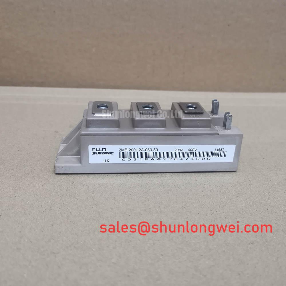
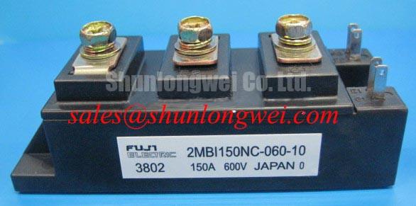
Benchtop Waveform Tuning: Mitigating Stress via Static and Dynamic Current Distribution on 2MBI150NC-060-10
Compare current in each parallel branch under the same operating conditions rather than judging balance from a single combined output-current trace. As a Design Consideration, static current sharing depends on the devices’ conduction characteristics and their temperatures, while dynamic sharing also depends on gate-loop impedance, switching delays, and the power interconnections. A cold-state diode check can support incoming screening, but it cannot predict either form of current sharing.
The temperature dependence of collector-emitter saturation voltage needs particular care. A positive temperature coefficient can support steady-state current sharing where the manufacturer’s characteristic curves establish that behavior at the relevant current and temperature. It should not be treated as an unconditional characteristic of the 2MBI150NC-060-10 across its entire operating range. For a parallel assembly, examine the applicable curves and compare branch currents as the mounting surfaces approach a stable temperature.
As an Engineering Recommendation, measure collector-emitter voltage with the same sensing arrangement on each branch. Differences in probe connection, contact resistance, and terminal voltage drop can otherwise look like differences between semiconductor devices. Record case temperature near comparable locations, and inspect the heatsink contact condition if current imbalance changes as the assembly warms. Consistent interface preparation and mounting pressure help make the comparison meaningful; tightening requirements belong to the module’s mechanical documentation, not a generic bolt-size assumption.
For dynamic balance, inspect the complete path from each driver output to its gate and back to the driver reference. Similar-looking wire lengths are not enough if one return path shares a high-current connection or passes beside a switching conductor. Symmetrical routing should include the outgoing and return conductors, comparable connection geometry, and consistent gate-resistor placement. The objective is to reduce unequal inductive feedback during switching, with the resulting balance established by measurements on the assembled circuit.
Capture the gate-emitter voltage and branch current together when comparing turn-on and turn-off behavior. Keep probe locations consistent and account for channel timing differences before interpreting an apparent switching mismatch. If the imbalance follows a measurement channel after probes are exchanged, investigate the measurement arrangement before changing the gate circuit. If it remains with the same branch, inspect that branch’s driver, interconnections, and thermal contact.
For replacement evaluation in a heavy-duty variable-frequency AC motor drive, compare the original assembly’s terminal arrangement, mounting envelope, cooling interface, and protection behavior. The related 2MBI100N-060-10 provides a separate model reference for a compatibility worksheet, not an assumed substitute. Similar naming does not establish interchangeable current capability, switching behavior, or mechanical fit.
Maintain a distinction between procurement identity and bench acceptance. The exact model suffix belongs on the inspection record, together with the applicable drawing revision and the equipment position being repaired. A module that passes a cold comparison still needs evaluation in the intended electrical and thermal conditions before the repaired assembly is returned to operation.
Transient Dynamics & Electrical Design: Mitigating Commutation Turn-Off Voltage Spikes on 2MBI150NC-060-10
Observe collector-emitter voltage at the module terminals during controlled switching tests, with a suitably rated differential probe and a measurement arrangement that minimizes pickup. As a Design Consideration, commutation-loop inductance contributes to turn-off voltage overshoot, while diode recovery can add current and ringing during the opposite switch’s turn-on. These effects require separate observations even when they appear within the same switching cycle.
Where the manufacturer’s circuit identifies an antiparallel freewheeling diode, evaluate its recovery behavior under the relevant current, temperature, and commutation conditions. Peak reverse-recovery current and the rate at which recovery current collapses influence switching stress, but neither can be inferred from a satisfactory diode-range reading. The meter supplies a low-energy static check; an operating waveform reveals the interaction between the diode, the switching device, and the surrounding circuit.
As an Engineering Recommendation, correlate the recovery-current trace with the opposing device’s gate waveform and collector-emitter voltage. An abrupt recovery transition can excite the commutation loop, but ringing alone does not identify the diode as the sole cause. Probe pickup, busbar geometry, capacitor connections, and gate-drive behavior can produce similar-looking features. Compare the timing of these signals before assigning a corrective action.
Turn-on gate resistance and an RC snubber are system-level adjustment options, not fixed accessories or prescribed values for this module. Increasing gate damping can alter switching speed and losses; a snubber introduces its own dissipation and component stresses. The appropriate approach is to identify the dominant transient, make a controlled change, and compare voltage peaks, current peaks, switching energy, and temperature under equivalent conditions. Component values should follow the measured circuit behavior and the equipment’s operating requirements.
Busbar symmetry matters when modules operate in parallel because unequal power-loop inductance can create unequal transient voltage and current stress. Keep the electrical geometry comparable between branches and examine the connections to the local DC-link capacitors. This addresses dynamic balance; it does not replace the conduction-characteristic and temperature checks needed for steady-state sharing. Treating both problems as a gate-resistor adjustment can conceal a mechanical or power-interconnection mismatch.
Dead-time verification belongs in the same waveform review. As a Design Consideration, compare the actual gate-emitter transitions of complementary switches rather than relying only on the controller’s commanded timing. Driver propagation delays, gate discharge behavior, and switching-node movement can change the effective separation between conduction intervals. The equipment designer should establish timing from measured behavior across the intended conditions without adding an arbitrary delay that increases unwanted diode conduction.
If the equipment uses desaturation protection, assess detection, blanking, and controlled turn-off as a coordinated sequence. A low-energy incoming test does not establish short-circuit withstand capability, and a normal conduction-voltage reading does not validate the protection circuit. Review the applicable device limits and capture the driver’s response using an approved test method. The IGBT Design & Integration guide provides broader context for gate-drive, thermal, and topology interactions without replacing the model-specific specification.
Topology references also need clear boundaries. Fuji Electric’s PIM (Power Integrated Module) 7-Pack information concerns a different integrated module category; it should not be used to infer rectifier, brake-switch, or terminal functions for this part. Establish those functions from the exact circuit diagram before planning a fixture or replacement connection.
Benchtop Waveform Tuning: Mitigating Stress via Auxiliary Emitter Return Trace Separation on 2MBI150NC-060-10
Trace the driver’s emitter-reference connection from the schematic to the physical terminal before modifying the return wiring. An auxiliary or Kelvin emitter connection must be explicitly identified in the module documentation; the package designation alone does not establish that such a terminal exists. This distinction prevents a general gate-layout technique from becoming an unsupported claim about the internal construction of the 2MBI150NC-060-10.
As a Design Consideration, shared emitter-path inductance creates a voltage contribution when power current changes rapidly. If the driver references its gate output through that same path, the contribution changes the effective gate-emitter voltage seen by the switching device. An emitter return separated from the main current path can reduce this coupling where the terminal arrangement supports it. The practical objective is reduced common impedance, not simply adding another conductor.
Where a dedicated auxiliary emitter is documented, route its driver return with the gate conductor and keep the pair away from the main commutation loop. Where the documented arrangement provides no dedicated auxiliary connection, review the external driver-reference takeoff and avoid unnecessary shared power-current routing. Either arrangement must respect the actual terminal functions; a convenient spare-looking terminal is not evidence of an emitter-sense connection.
During waveform inspection, measure gate-emitter voltage at the relevant module connections rather than only at the driver-board output. Differences between those locations can reveal the effect of the interconnect. Use short, appropriate probe connections and inspect the waveform during both switching directions. A ringing trace may indicate coupling or inadequate damping, but it should be compared with collector-emitter voltage and current before deciding whether the gate loop is responsible.
Clearance and insulation checks should follow the physical return-path review. As an Engineering Recommendation, inspect contamination, damaged barriers, terminal spacing, and cable movement against the equipment’s insulation-coordination requirements. The semiconductor’s 600 V rating is not an insulation-withstand test specification. For a dielectric test, establish the specified terminal grouping, baseplate connection, waveform, duration, and acceptance criteria from the applicable manufacturer and equipment procedures.
Before an insulation test, separate connected electronics that are outside the approved test configuration and ensure that semiconductor terminals are grouped as required by that procedure. A test applied between the wrong nodes can stress semiconductor junctions instead of evaluating the intended insulation barrier. Record the fixture connections with the result so a later inspection can reproduce the same test rather than compare unrelated measurements.
Complete the wiring correction by repeating the gate-reference measurement under the same conditions used before the change. Compare switching behavior, driver-reference movement, and protection response, then document the final return routing on the repair drawing. Acceptance should rest on repeatable measurements at the module terminals, with the installed connections matching the verified schematic.