
Content last revised on October 9, 2026
Initial Inspection and Rating Verification
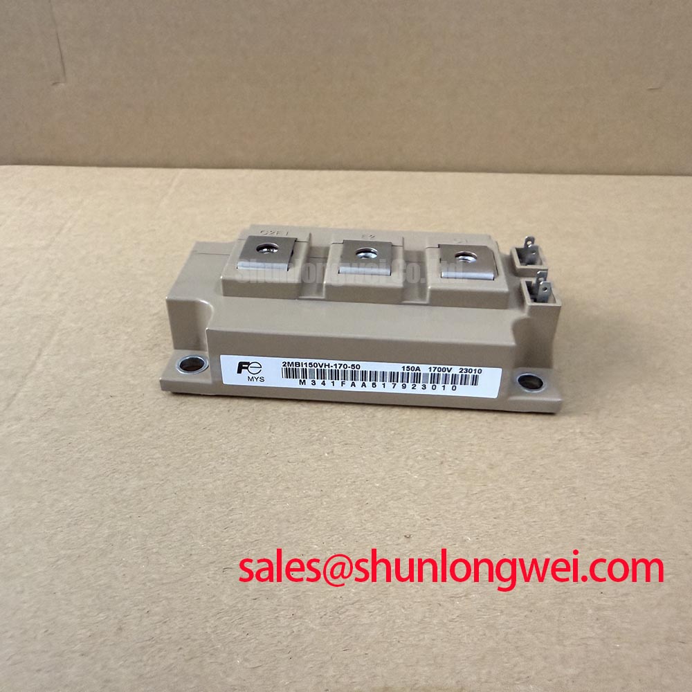
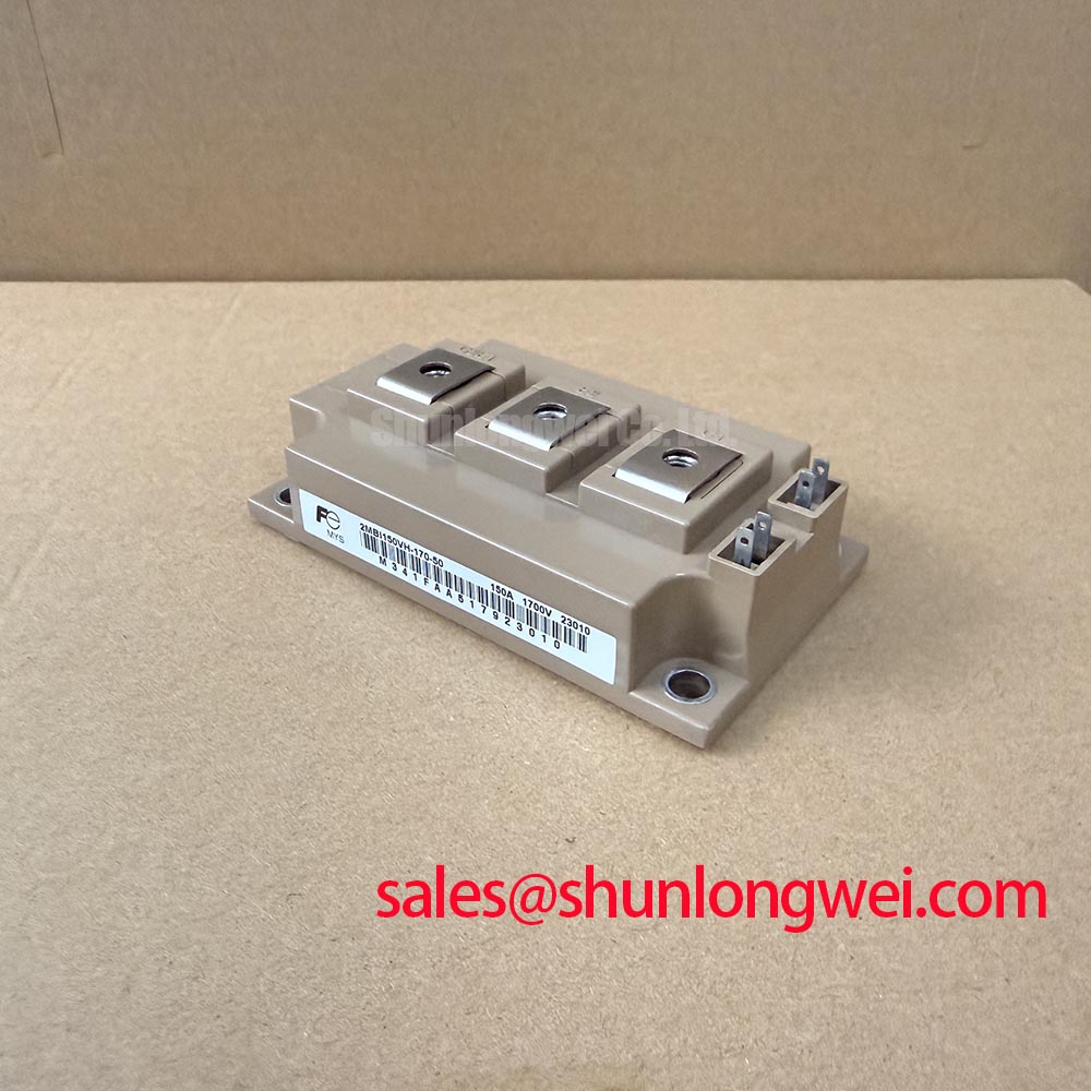
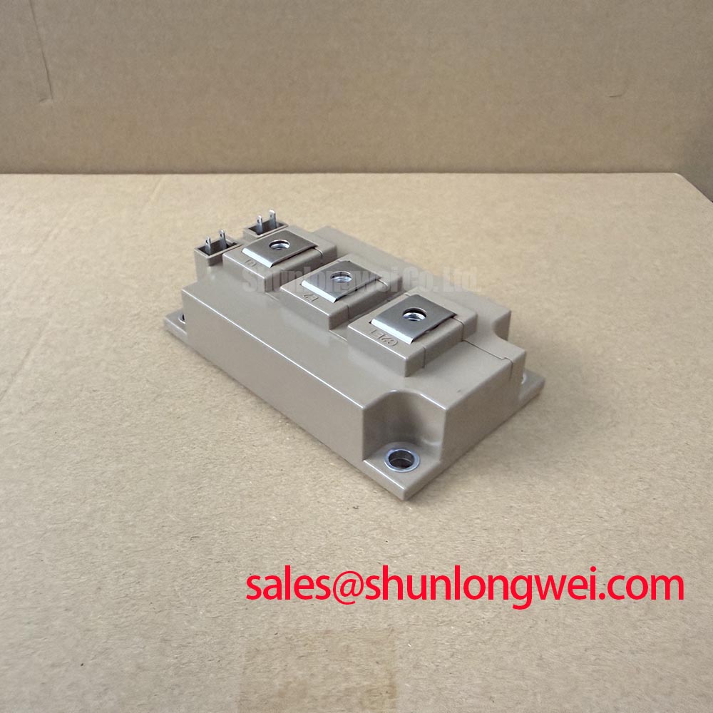
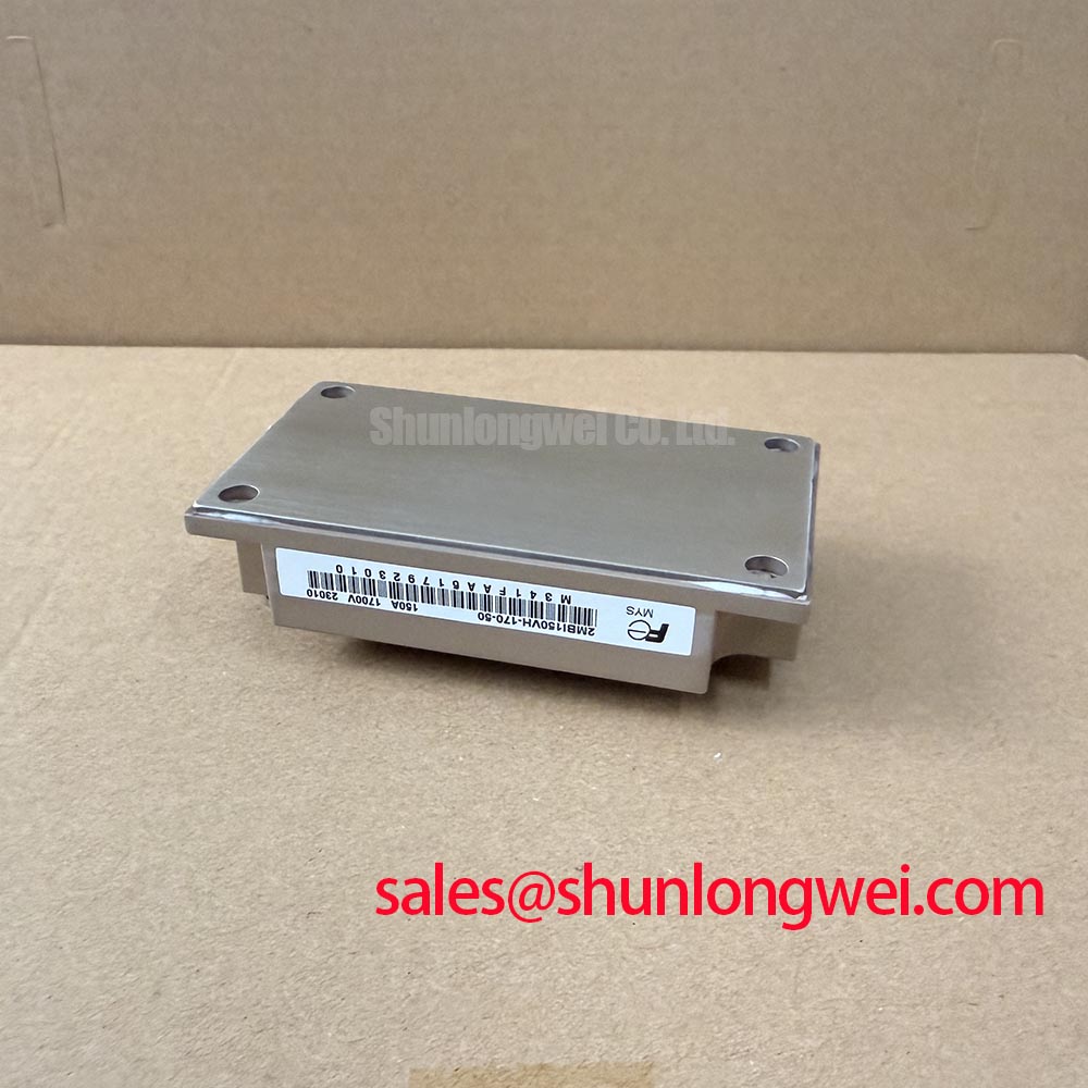
With the traction inverter isolated and its DC link verified discharged, check the 2MBI150VH-170-50 marking against the equipment parts list, then confirm terminal polarity from the manufacturer’s terminal drawing before making resistance or diode-mode measurements. Record the module temperature and meter settings so that incoming inspection results remain comparable between units.
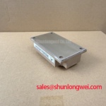
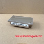
The Fuji Electric 2MBI150VH-170-50 is an IGBT module with the electrical limits below. For high-speed rail or heavy freight locomotive traction inverter maintenance, these ratings support an initial compatibility review; they do not establish railway qualification, inverter compatibility, or permissible operating conditions by themselves.
| Parameter | Official Specification | Interpretation for inspection |
|---|---|---|
| Collector-emitter voltage, VCES | 1700 V | Device voltage rating, not a recommended DC-link operating voltage. |
| Continuous collector current, IC | 150 A at Tc = 80 °C | Current rating with the stated case-temperature condition. |
| Gate-emitter voltage, VGE | ±20 V | Gate voltage limit, not a gate-driver supply recommendation. |
| Short-circuit withstand time, tsc | ≥10 µs | Requires the manufacturer’s associated test conditions and protection limits. |
| Package | M239 | Use the package drawing to verify mounting and terminal compatibility. |
Optimizing Heatsink Contact Pressure and Surface Roughness for Minimum Rth(c-s)
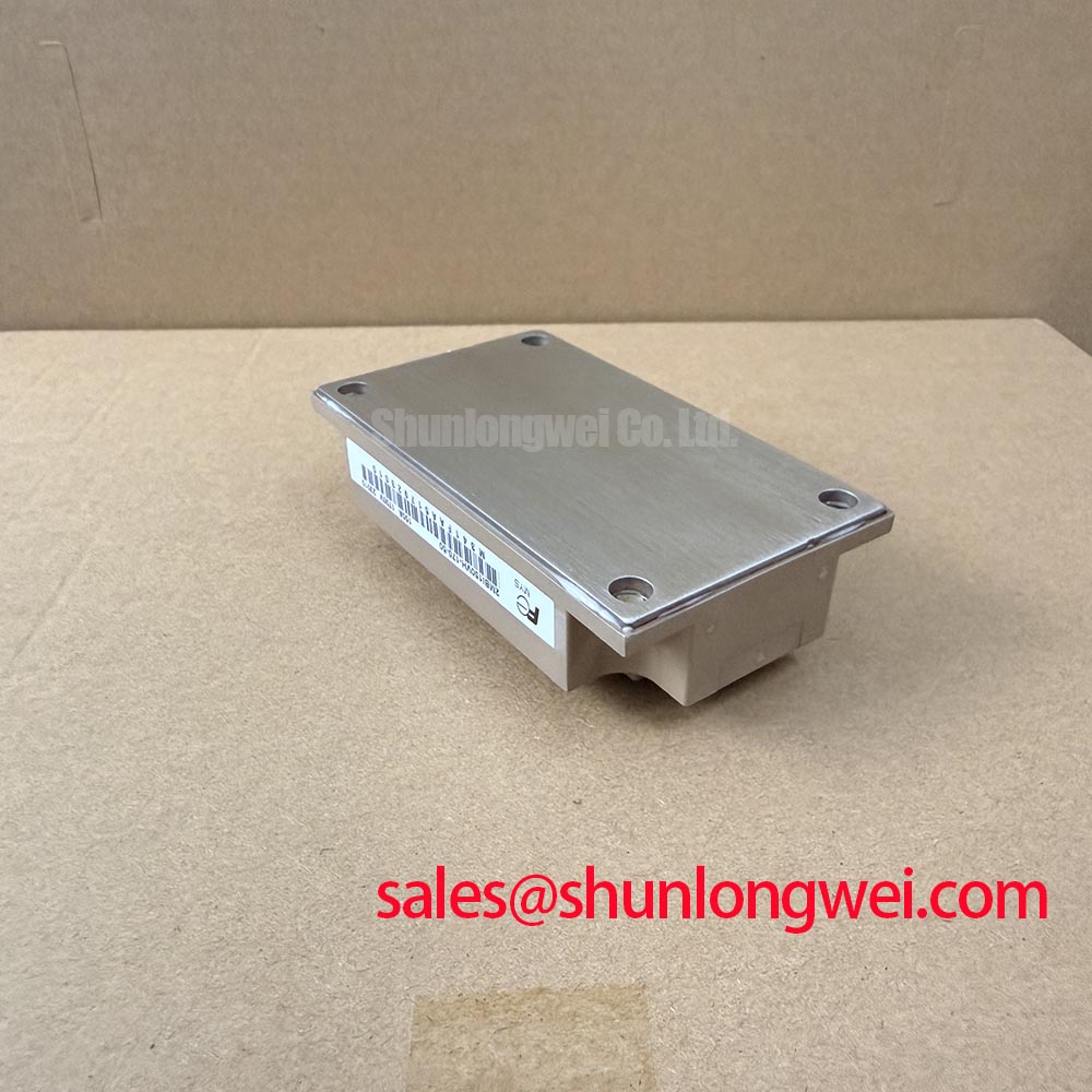
Inspect the heatsink contact face before installing the M239 package. Remove residual interface material without scratching the mating surface, then check for burrs, embedded particles, corrosion, and distortion around mounting holes. A module that appears seated can still have uneven thermal contact if a raised edge or trapped particle carries the mounting load. Treat surface preparation and contact assessment as Design Considerations, not as evidence of a particular thermal resistance.
Thermal interface material should fill surface irregularities without creating an unnecessarily thick thermal barrier. Its application thickness, coverage pattern, and compatibility should follow the selected material’s instructions and the module mounting guidance. The available specifications do not establish a numerical thickness target, surface-roughness limit, or mounting torque for this model. During assembly validation, inspect the contact imprint for uncovered regions and excessive accumulation; an imprint is useful evidence of distribution, but it is not a calibrated measurement of thermal resistance.
Check baseplate flatness against the applicable drawing and mounting instructions rather than attempting to compensate for curvature through extra screw force. Tightening in a controlled sequence can help distribute loading, but the sequence and final torque need to come from the approved assembly procedure. Do not infer press-pack construction, disc-spring loading, or double-sided cooling from the M239 designation.
When a repaired traction inverter shows uneven heating, compare case-temperature measurements under equivalent loading and inspect both the interface and cooling path. Blocked airflow, coolant restrictions, sensor placement, and unequal electrical losses are alternative explanations. The 150 A at 80 °C case temperature rating does not mean that continuous operation at that current is acceptable regardless of switching loss or cooling performance.
High-Frequency Commutation Loop Inductance Minimization in High-Power Arrays
Trace the commutation path through the DC-link capacitor, power terminals, and switching devices before evaluating an existing busbar assembly. As a Design Consideration, reducing enclosed loop area and maintaining closely coupled outgoing and return paths can reduce parasitic inductance. Symmetry also helps when assessing current distribution in arrays, although a visually symmetrical assembly is not proof of balanced switching behavior.
An Engineering Calculation expresses the inductive contribution to collector voltage as Vpeak ≈ VDC + Lσ(di/dt). This simplified relationship explains why faster current change can raise turn-off overshoot even when the DC-link voltage remains unchanged. It does not capture every ringing or distributed-circuit effect. Measure the switching waveform using an appropriately rated probe and a low-inductance measurement connection, then assess the peak against the 1700 V device rating with margins determined by the inverter design.
Snubber capacitance, damping, and placement should be selected from measured parasitics, switching energy, and component temperature rise. No fixed loop-inductance target or switching-frequency range is established by the supplied module specifications. At higher switching frequencies, review total device losses and cooling capability rather than extrapolating the continuous-current rating. In a locomotive cabinet, also verify that the cooling arrangement performs under the equipment’s specified ambient and contamination conditions.
During diode-mode inspection, record polarity and the repeatability of each accessible conduction path. A handheld meter’s forward-voltage reading is not a reverse-recovery measurement and cannot establish diode softness, surge-current capability, or operating-temperature behavior. Reverse-recovery current can affect commutation overshoot and electromagnetic emissions; evaluate it dynamically under relevant circuit conditions rather than assigning an unsupported softness factor to this module.
Long motor cables introduce another voltage-stress mechanism: traveling-wave reflections at the motor terminals. Separate those measurements from module collector-emitter measurements, and assess any output filter against the cable, motor insulation, and inverter requirements. Do not assume a universal voltage multiplier. Fuji Electric’s High-Speed Discrete IGBTs resource provides related manufacturer context, but discrete-device characteristics must not be transferred to this module.
High-Speed Fault Management: VCE(sat) Desaturation Sensing Circuitry
For incoming inspection, compare collector-emitter leakage behavior and gate-emitter impedance using an approved, current-limited procedure. In-circuit readings may include driver resistors, protective devices, and parallel conduction paths, so investigate unexpected results before attributing them to the module. A gate-threshold measurement requires controlled collector current, voltage, and temperature; without the manufacturer’s test conditions and limits, a measured threshold cannot support a numerical pass-or-fail decision.
💡 Bench Tip: Keep the gate under ESD-controlled handling and prevent it from floating during cold-state diode checks, because stored gate charge can change the apparent collector-emitter conduction state.
The stated short-circuit withstand time of ≥10 µs is not permission to hold a fault for that duration. Protection coordination requires the associated gate voltage, supply voltage, temperature, and short-circuit test conditions. Review the complete interval from fault initiation through sensing, propagation, driver response, and current extinction. Both a fault present at turn-on and a fault developing during conduction warrant evaluation against the manufacturer’s applicable operating limits.
Desaturation sensing should distinguish normal switching transitions from excessive collector-emitter voltage during commanded conduction. Blanking behavior, sensing-path coupling, and the driver’s fault response are system-dependent. A staged or controlled turn-off may reduce inductive overshoot, but its timing and gate-current profile require waveform validation. Confirm that the opposite switch remains inhibited during fault handling.
A semiconductor fuse provides a separate protection function and does not replace fast gate-driver fault management. Compare prospective fault current, DC interrupting capability, let-through energy, and clearing behavior with documented circuit limits. The general explanation of semiconductor high-speed fuse protection is useful background, not proof of protection coordination for this module. No module-specific surge-current or energy limit supplied here supports a claim of rupture prevention. For measurement-led troubleshooting, the Field Engineer’s Handbook provides a complementary diagnostic reference.
Common-Mode Transient Immunity in Harsh Industrial Environments
Inspect the gate-driver isolation boundary, connector routing, and spacing around power terminals before energized testing. Common-mode transient immunity is a property of the relevant driver or isolation component under specified conditions; it is not established by the module’s collector-emitter voltage rating. Likewise, the supplied specifications provide no numerical isolation-test voltage or reinforced-insulation classification for this module.
As a Design Consideration, assess clearance and creepage using the equipment’s working voltage, insulation architecture, pollution conditions, and applicable standards. Keep conductive debris and interface material away from insulating surfaces. Any dielectric withstand test should follow the approved voltage, duration, terminal grouping, and equipment procedure; an improvised high-voltage bench test cannot establish insulation reliability.
If an inverter records unexpected switching events, correlate gate-emitter voltage, driver supply behavior, and fault signals before identifying a cause. Observe the gate relative to its associated emitter with suitable measurement equipment. Coupled noise, driver supply disturbance, and measurement artifacts can produce similar observations, so compare against a known-good channel under equivalent conditions.
For replacement assessment, compare the exact 2MBI150VH-170-50 designation, terminal arrangement, mounting drawing, driver requirements, and thermal limits with the equipment documentation. The related 2MBI400VB-060-50 can be included in a cross-model review, but family resemblance does not establish electrical or mechanical interchangeability. Resolve discrepancies before installation rather than treating a matching product category as replacement approval.

