

Content last revised on September 13, 2026
Field Diagnostics & Commissioning: Auxiliary Emitter Return Trace Separation in 2MBI200S-120 Topologies
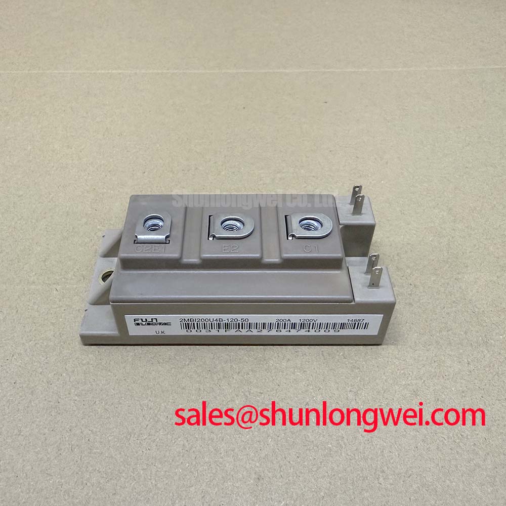
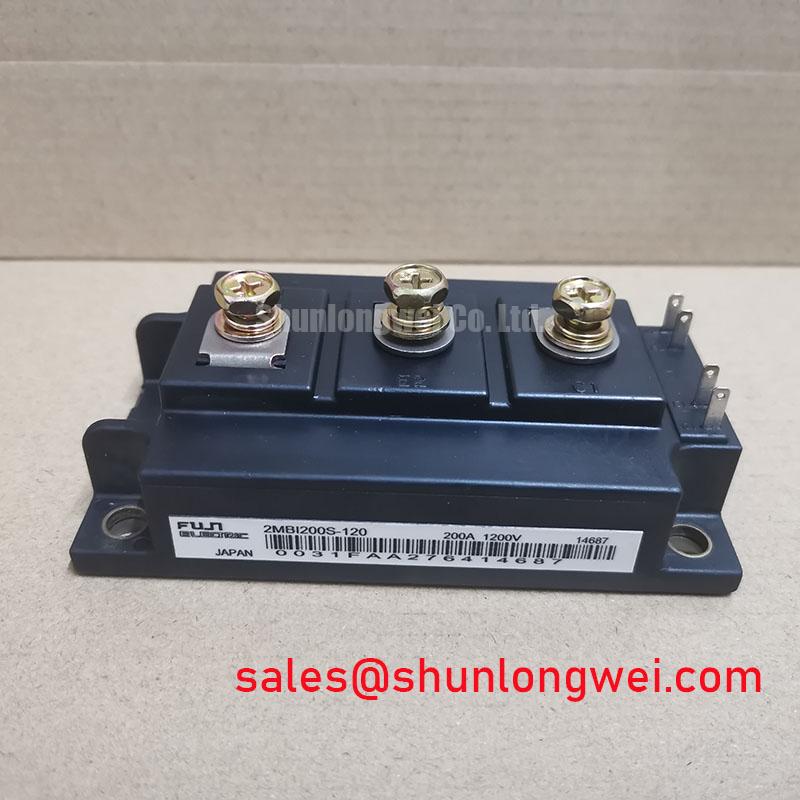
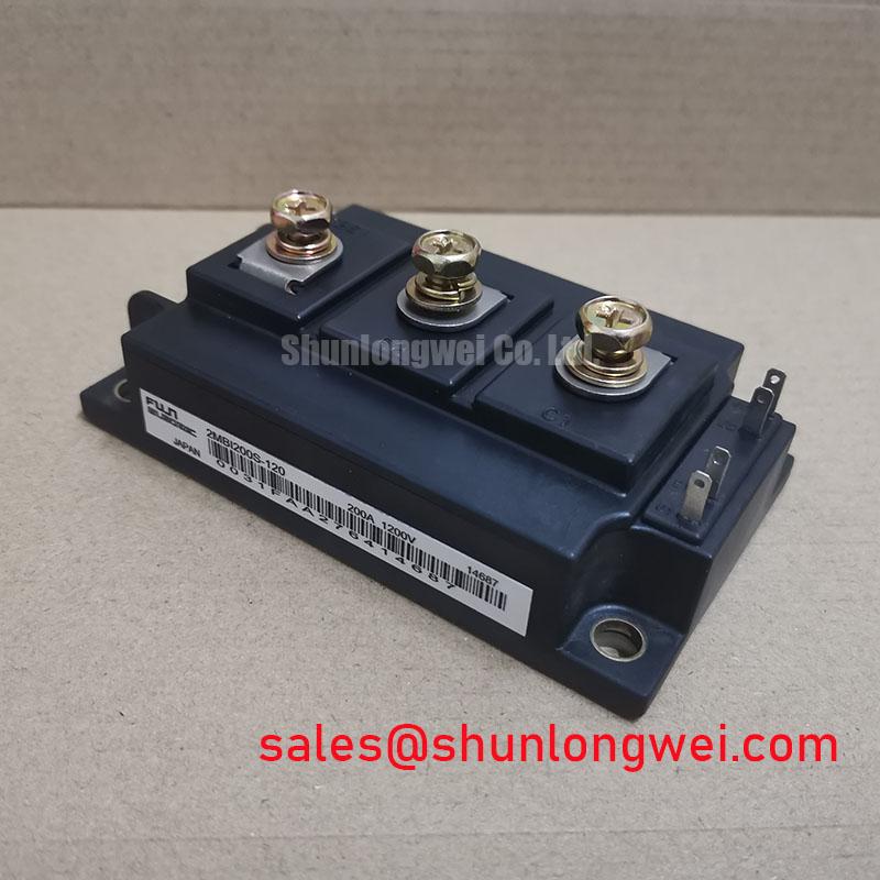
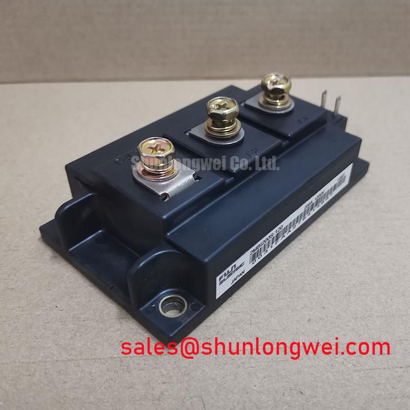
Start a field inspection by identifying the collector, emitter, gate, and auxiliary emitter connections from the original Fuji Electric documentation and the equipment wiring diagram. Do not rely on terminal position alone when replacing a module in a populated inverter cabinet. Photograph the existing busbar arrangement, mark each conductor, and compare the replacement terminal pattern before applying pressure to the module terminals.
The auxiliary emitter return is used by the gate driver as a voltage reference. A high current emitter path carries switching current and develops a transient voltage across its unavoidable parasitic inductance. If that same path is shared with the gate driver reference, the driver can see an apparent gate voltage that differs from the voltage at the silicon die. This mutual coupling can appear as ringing, delayed turn off, uneven switching, or intermittent protection trips. Separating the auxiliary emitter return from the main power emitter path is therefore a sound Design Consideration when the module and gate driver provide that connection.
Keep the gate loop physically compact and route the gate and auxiliary emitter conductors together as a controlled pair wherever the equipment layout permits. Avoid routing the gate return beside a high di/dt collector bus, braking chopper connection, or commutation loop. The exact clearance and conductor geometry should be established from the insulation system, switching waveform, enclosure constraints, and applicable safety requirements rather than copied from a generic layout.
During commissioning, first test the gate driver with the power stage disabled. Confirm that the gate signal reaches the correct terminal and that the auxiliary emitter reference returns to the intended driver reference rather than to an arbitrary chassis point. Then inspect the signal with an oscilloscope using a measurement method suitable for the common mode voltage present in the converter. Look for excessive ringing, unequal rise and fall behavior, or a gate waveform that changes when the DC link is energized. These observations may indicate a return path or probe reference problem, but they do not identify a single failed component without comparison against a known good phase.
For a commercial string inverter or energy storage converter, the power return, gate return, current sensor wiring, and protective earth should be reviewed as separate functions. A low resistance reading between metalwork and a terminal does not confirm correct high frequency current routing. When the original assembly uses laminated busbars or dedicated driver boards, preserve the relative conductor arrangement during service. The 2MBI200UB-120 may be encountered in a related front end or auxiliary stage, but its presence does not establish interchangeability with this module; voltage, current, topology, terminal arrangement, and gate drive requirements must be checked independently.
Preventing Spurious Faults: Derating Guidelines and Mismatched Parameter Guidelines for 2MBI200S-120
The official electrical limits define the starting boundary for evaluation. The device is rated at Vces = 1200 V at Tj = 25°C, with Ic = 200 A at Tc = 80°C. Its collector emitter saturation voltage is specified as 2.2 V typical and 2.7 V maximum at Ic = 200 A, Vge = 15 V, and Tj = 25°C. The gate emitter voltage rating is ±20 V. These values should be read together with the actual DC link, switching transients, pulse duration, case temperature, and thermal impedance of the finished assembly.
| Parameter | Symbol | Condition | Official Specification |
|---|---|---|---|
| Collector emitter voltage | Vces | Tj = 25°C | 1200 V |
| Continuous collector current | Ic | Tc = 80°C | 200 A |
| Collector emitter saturation voltage | VCE(sat) | Ic = 200 A, Vge = 15 V, Tj = 25°C | 2.2 V typ., 2.7 V max. |
| Gate emitter voltage | Vges | Gate rating | ±20 V |
| Total power dissipation | Pc | Tc = 25°C, one device | 1040 W |
| Junction to case thermal resistance | Rth(j-c) | IGBT | 0.12 °C/W max. |
| Short circuit withstand time | tsc | Vcc = 600 V, Vge ≤ 15 V, Tj = 125°C | ≥10 µs |
| Maximum specified junction temperature | Tj | Maximum rating | +150°C |
The positive temperature coefficient associated with the stated saturation voltage can support static current sharing between parallel semiconductor paths, but it does not remove the need for symmetrical gate loop wiring. Dynamic sharing is strongly influenced by gate resistance, driver propagation delay, common emitter inductance, busbar geometry, and the switching state of the other devices. When evaluating parallel operation, engineers should measure each gate emitter waveform and collector emitter transient under the intended load instead of assuming that equal nominal ratings produce equal dynamic current.
Parameter mismatch can also arise when a service replacement is selected by voltage and current alone. Compare the package outline, terminal sequence, internal circuit arrangement, gate charge information, diode or complementary path data where applicable, and the thermal interface to the original design documentation. The 2MBI150UC-120 is a related Fuji Electric part that may be reviewed during cross model evaluation, but it should not be treated as a drop in substitute without a complete electrical and mechanical compatibility review.
Inspect creepage and clearance around the module, busbar supports, driver connectors, and insulating barriers. The required distances are determined by working voltage, overvoltage category, pollution environment, altitude, insulation material, and the governing equipment standard. A replacement that fits the screw holes can still be unsuitable if the original spacing or insulation coordination is changed.
For vibration exposed cabinets, check that busbars are supported independently of the module terminals and that fasteners cannot loosen under thermal cycling. Torque is a mechanical assembly requirement governed by the fastener, thread, washer, busbar, and manufacturer instructions. ⚠️ Field Alert: Disconnect and verify the absence of hazardous voltage before inserting, removing, or tightening any module or gate driver connection.
Assembly Integrity & Layout Architecture: Implementing Galvanic Gate Drive Isolation, Reinforced for 2MBI200S-120
Where galvanic isolation is used, the gate driver must maintain a controlled isolation barrier between the control domain and the switching power domain. For a proposed reinforced barrier, the system designer should verify the required withstand voltage, creepage, clearance, insulation classification, partial discharge behavior, and common mode transient immunity from the selected isolator and the complete driver assembly. Values such as a barrier above 5 kV or CMTI above 100 kV/µs must not be attributed to the IGBT module unless they are explicitly stated in the relevant component documentation.
At the module interface, keep the isolated driver supply, gate resistor network, gate conductor, and auxiliary emitter return arranged to limit the area exposed to the collector switching field. Minimize parasitic loop inductance as a layout principle to suppress turn off overshoot and unwanted gate voltage movement. The system engineer must verify peak gate and collector emitter margins during switching tests at the intended DC link voltage, load current, temperature, and protection state.
When a bootstrap supply is used for a high side gate driver, the bootstrap capacitor must retain adequate charge during the high side on time, while the charging diode and driver supply must tolerate the required repetition rate and voltage transition. The correct capacitance, charging current, diode recovery behavior, and refresh interval are system determined. Confirm these items against the driver data sheet and the converter timing rather than assigning a universal capacitor value to the 2MBI200S-120.
Spurious turn on can be investigated by monitoring the gate emitter voltage during the opposite switch transition and by checking whether the isolated driver supply dips or shifts relative to its local reference. A fault that appears only at high bus voltage may involve common mode coupling, probe technique, insulation displacement, driver saturation, or busbar resonance. Compare phase legs under identical test conditions and inspect the isolation barrier for contamination or unintended conductive paths.
Fuji Electric provides broader application context through its 7th Gen X Series IGBT Modules information and its RC IGBT Modules information. Those product families should be treated as technical references for their own devices, not as evidence that every feature or rating applies to the 2MBI200S-120.
2MBI200S-120 Operational Boundaries: Evaluating Thermal Capacitance vs Heat Sink Limits
Thermal evaluation begins with the official Rth(j-c) of 0.12 °C/W maximum for the IGBT, the 1040 W total power dissipation at Tc = 25°C for one device, and the +150°C maximum specified junction temperature. These values do not by themselves predict operating temperature in an inverter. Switching loss, conduction loss, pulse profile, case temperature, thermal interface quality, heat sink impedance, airflow, coolant condition, and neighboring heat sources all contribute to the actual junction temperature.
For a pulsed overload, the heat sink cannot be represented as an instantaneous temperature clamp. The case and heat sink absorb energy over time, so the junction temperature response depends on the transient thermal impedance curve and the pulse sequence. A multi RC thermal model can be used as an Engineering Calculation method: determine the electrical loss waveform, apply each pulse to the manufacturer’s transient thermal data, and combine the resulting junction rise with the measured case temperature. The calculation should then be checked against thermocouple or suitable infrared measurements at the case and against switching waveform data.
Do not use the short circuit withstand figure as an invitation to operate continuously in a fault state. The official condition is tsc ≥10 µs at Vcc = 600 V, Vge ≤15 V, and Tj = 125°C. Actual protection performance depends on desaturation detection, driver propagation delay, blanking time, gate discharge path, fault coordination, DC link conditions, and the inductance in the fault loop. Commissioning should verify that the protection sequence interrupts the fault within the validated system boundary.
The thermal interface should be clean, continuous, and compatible with the module baseplate and heat sink finish. Apply thermal compound as a thin, even interface layer according to the compound and equipment instructions; excessive compound can increase mechanical contamination without improving heat transfer. The mounting sequence should keep the baseplate flat against the heat sink, with fastener tightening performed progressively and checked against the applicable assembly specification.
Regenerative braking and energy storage applications deserve a separate loss review. A braking chopper can impose repetitive current pulses through the IGBT while the resistor absorbs the returned energy. Select the resistor, chopper duty cycle, overload profile, cooling arrangement, and fault protection from the measured energy and thermal cycle of the complete system. The module’s current and voltage ratings are necessary limits, not a substitute for validating resistor energy absorption, DC link overvoltage control, and switching loss.
High altitude, cosmic ray exposure, single event burnout, FIT values, service life, and insulation reliability require application specific evidence from the manufacturer, qualification reports, or recognized standards. Without such a source, these subjects remain Design Considerations; no numerical failure rate or lifetime claim should be assigned to this module. For practical troubleshooting and broader system reliability context, engineers can consult the Power Electronics Masterclass while validating the final design with equipment level testing.
Before returning a repaired converter to service, record the cold terminal inspection, gate waveform, DC link transient, case temperature, protection response, and fastener condition. The acceptance limits should come from the original equipment documentation and the system safety assessment, with the 2MBI200S-120 official ratings used as the component boundary.