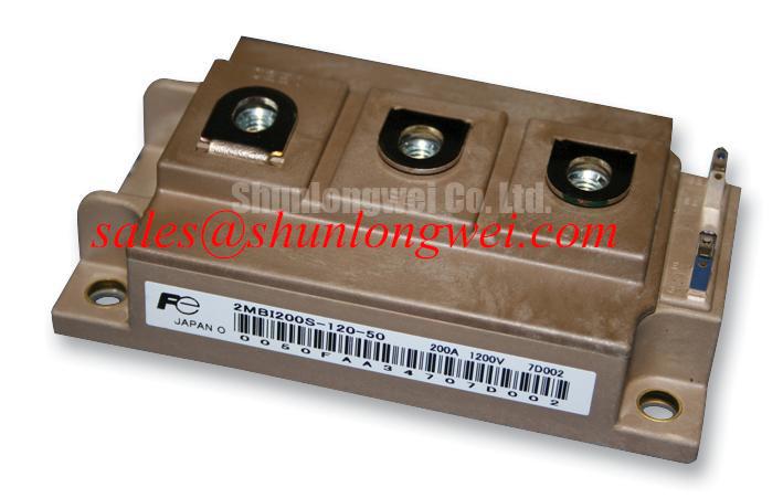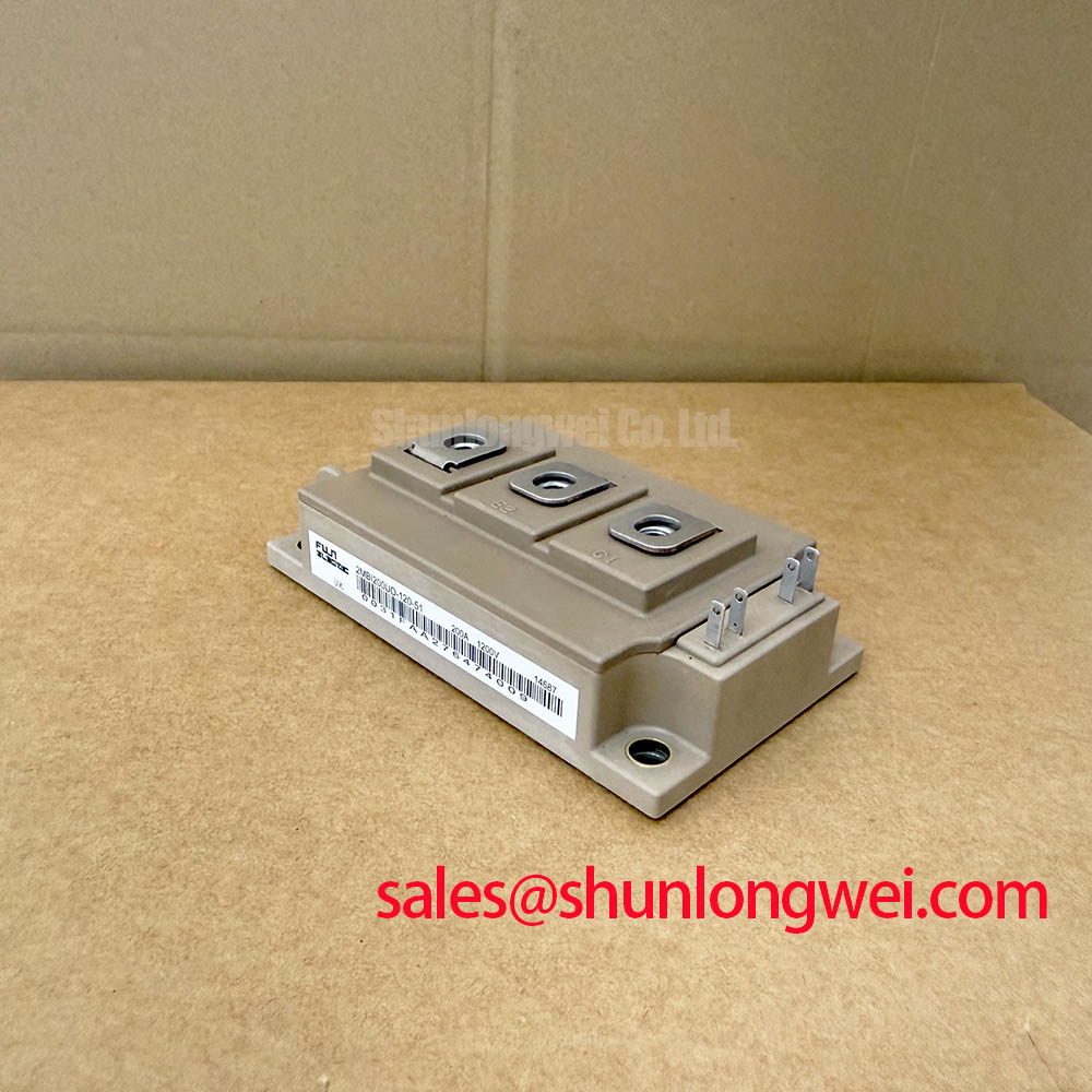
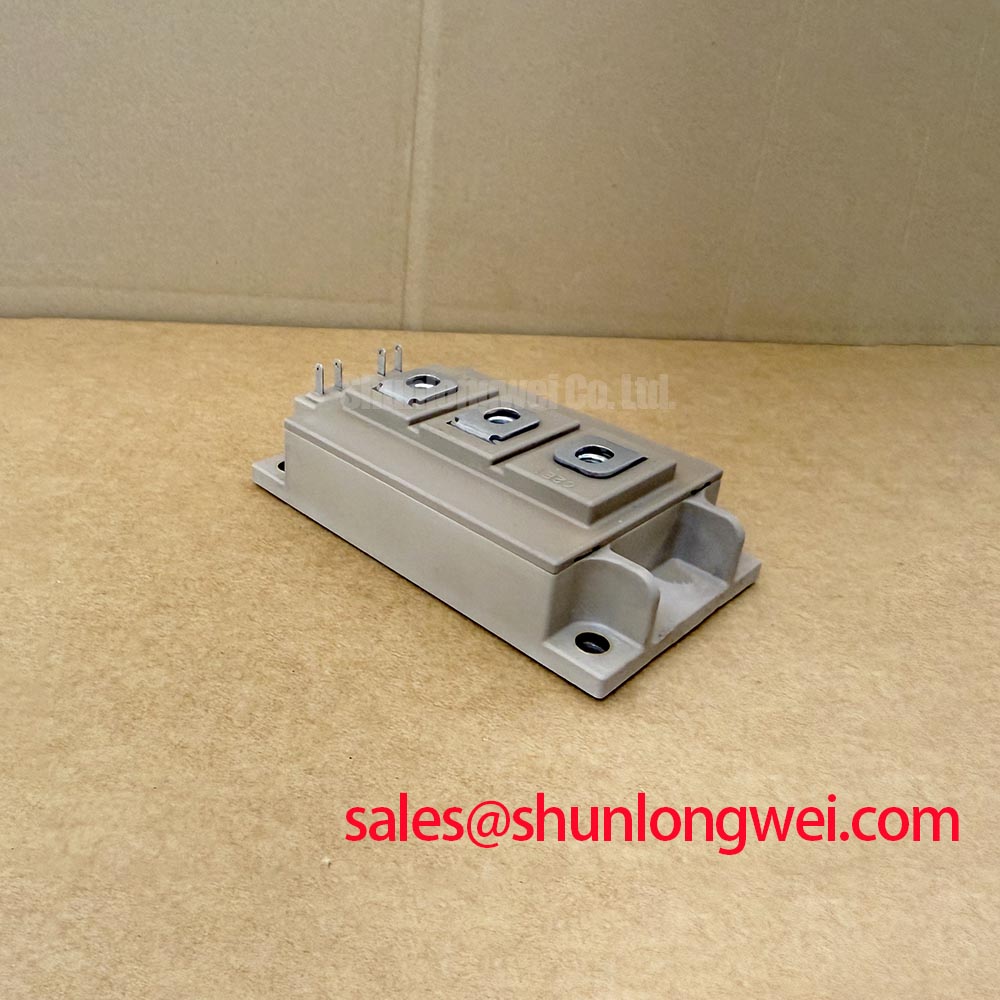
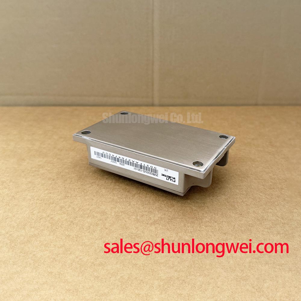



Content last revised on September 10, 2026
2MBI200UD-120-51 Circuit Protection & Reliability: Calibrating Thermal Stress Alleviation in Bidirectional Power Flow
| Manufacturer | Fuji Electric |
|---|---|
| Product Category | IGBT Module |
| Collector-Emitter Voltage | 1200V VCES Official Datasheet Specification |
| Collector Current | 200A IC at TC = 25°C Official Datasheet Specification |
| Saturation Voltage | 2.20V VCE(sat) Official Datasheet Specification |
| Turn-Off Time | 1.0µs maximum toff Official Datasheet Specification |
| Isolation Voltage | 2500V AC VISO Official Datasheet Specification |
Record heatsink temperature, airflow condition, terminal contact temperature, and inverter current traces before replacing a 2MBI200UD-120-51 module in a bidirectional power stage. This establishes whether the fault developed during sustained load, repeated battery charge and discharge transitions, or a thermal cycling event caused by intermittent cooling performance.
The Fuji Electric module is rated at 1200V VCES and 200A IC at TC = 25°C, both Official Datasheet Specifications. These ratings support engineering evaluation in industrial DC-link systems associated with commercial string inverters and micro-grid energy-storage equipment. The module’s 2.20V VCE(sat) is also an Official Datasheet Specification and is relevant when assessing conduction loss during high-current intervals. Actual operating loss depends on current waveform, gate-drive behavior, switching frequency, cooling conditions, and the surrounding power topology.
In battery-linked inverter equipment, active power can reverse direction between the DC battery rack and the AC inverter link. That reversal can change which devices conduct, which diodes recover, and where the dominant heat appears in a power assembly. A stable average heatsink temperature does not automatically indicate stable semiconductor stress. Repeated charge-discharge duty can create temperature swings at the module interface and across its electrical connections, particularly where airflow is restricted or thermal interface material has hardened with age.
Design Consideration: inspect the complete thermal path rather than treating the IGBT module as an isolated source of heat. Check the heatsink for dust accumulation, verify that cooling fans reach normal speed, inspect air passages for blockage, and examine the mounting surface for corrosion, scratches, or uneven clamping marks. A clean and flat interface supports repeatable heat transfer; the system thermal design must determine whether measured temperatures remain within its intended operating limits.
Use the original mechanical documentation to confirm the correct mounting hardware, tightening sequence, and torque. Uneven fastening can introduce local thermal resistance even when the module remains electrically functional. Apply thermal interface material as a controlled, continuous layer rather than allowing dry zones or excess material to collect around mounting areas.
⚠️ Maintenance Note: Monitor terminal contact temperature during loaded operation and recalibrate terminal tightness and cooling-airflow checks as part of scheduled preventive maintenance.
The 2500V AC VISO rating is an Official Datasheet Specification for isolation between the module’s power and control circuits. It does not define creepage distance, clearance, enclosure insulation performance, cable insulation, or the insulation coordination of the finished inverter. Design Consideration: keep power conductors, gate-drive wiring, sensing wiring, and chassis-connected structures arranged according to the insulation requirements of the completed system, especially where moisture, dust, salt residue, or condensation can reduce surface insulation performance.
For general power-semiconductor context, Fuji Electric presents its power semiconductor and IPM module portfolio. When evaluating a replacement event, preserve the original power-stage topology, gate-drive architecture, cooling interface, and protection strategy instead of relying on voltage and current ratings alone.
Field Diagnostics & Commissioning: DC-Link Capacitance Bank Layout and Low-ES in 2MBI200UD-120-51 Topologies
Capture collector-emitter voltage and phase-current waveforms at the module terminals during controlled switching tests to identify overshoot, ringing, and asymmetric commutation behavior. A measured voltage peak is influenced by the DC-link voltage plus the voltage produced by stray inductance and current-transition rate. In practical terms, the relationship follows Vpeak = VDC + Lsigma multiplied by di/dt, so both wiring geometry and switching behavior must be examined together.
The 1.0µs maximum turn-off time is an Official Datasheet Specification for the 2MBI200UD-120-51. It is relevant to dead-time review and protection timing analysis, but it is not a complete switching-loss or commutation specification for an assembled inverter. Probe placement, current level, temperature, gate resistance, parasitic inductance, and the response of the associated freewheeling path all affect observed switching behavior.
Design Consideration: position the DC-link capacitor bank so the switching-current path is physically compact and has low parasitic inductance. A symmetrical laminated or planar busbar arrangement can help reduce loop area, provided the final arrangement is verified by switching tests at the actual DC-link voltage and operating current. Long conductors, offset capacitor connections, and unequal parallel paths can produce ringing that is visible even when static resistance measurements appear acceptable.
Where turn-off ringing is present, inspect capacitor connections, busbar joints, terminal hardware, and the layout path from the DC-link capacitor bank to the IGBT module. Check for loose fasteners, heat-discolored metalwork, damaged insulating barriers, and conductor routing that separates outgoing and return current paths. The corrective action should be determined from measured voltage and current waveforms rather than from a generic component value.
Freewheeling diode reverse recovery can affect the sharpness of the commutation transient and the spectral content of conducted and radiated noise. A rapid recovery event can interact with loop inductance and create high-frequency ringing; a smoother waveform may indicate a different balance of switching loss and transient behavior. Engineering Recommendation: compare the affected phase leg with a known-good leg using the same probe method and loading condition. This helps distinguish a layout issue, a gate-drive asymmetry, a degraded DC-link connection, or a load-related event.
Metal-oxide varistors and snubber networks are system-level overvoltage-control elements rather than intrinsic specifications of this Fuji Electric module. Their location, energy capability, and coordination with capacitors and gate-drive timing must be selected for the actual fault energy and measured transient conditions. They should not be treated as a substitute for a short and balanced DC-link current loop.
In systems with a separate rectifier or auxiliary power-conversion section, engineers may also encounter modules such as the 3MBI50SX-120-02. Its electrical role, package arrangement, and drive requirements must be assessed independently; it should not be assumed to be interchangeable with the 2MBI200UD-120-51.
Benchtop Waveform Tuning: Mitigating Stress via Optocoupler vs Digital Coreless Transformer on 2MBI200UD-120-51
Compare the commanded gate signal with the voltage measured at the module gate reference during each switching edge, because a clean controller output can still arrive at the module with distortion, delay, or unintended coupling. This check is especially important after replacing a power module, repairing a driver board, changing cable routing, or correcting a DC-link connection.
The module’s 2500V AC isolation voltage is an Official Datasheet Specification for the power-to-control isolation boundary within the device. A gate-driver isolation system has its own separate insulation, transient-immunity, power-supply, and layout requirements. Do not infer a driver’s reinforced-isolation classification or common-mode transient immunity from the module’s VISO rating.
Optocoupler-based and digital coreless-transformer gate-drive interfaces require different validation methods. The useful field question is not which method is universally preferable, but whether the installed driver preserves a stable off-state and a repeatable switching transition under the converter’s actual common-mode voltage movement. Observe gate behavior while the corresponding phase leg switches under controlled load. A gate waveform that moves unexpectedly during the opposite device transition may indicate common-mode coupling, shared-return impedance, probe-reference error, or gate-driver output imbalance.
Design Consideration: route gate-drive conductors as compact paired paths and keep sensitive driver-side signals segregated from high-current power paths. This reduces magnetic and capacitive coupling that can alter apparent gate behavior. The final acceptable waveform, switching speed, and noise margin must be established by the system engineer through measured testing with the intended driver, DC-link layout, load, and protection circuit.
Check that the oscilloscope probe method does not create a false return path or expose the operator to the high-energy DC link. Differential measurement equipment and a controlled test arrangement are appropriate where switching nodes cannot be referenced safely to bench earth. If results change sharply when the probe position changes, repeat the measurement using a verified reference method before modifying gate components.
Inspect the driver supply rails during switching, not only while idle. Supply droop, damaged local decoupling, connector oxidation, or an unstable isolated supply can affect both the on-state command and the ability of the driver to hold the device off. If a repaired unit uses plug-in control wiring, reseat connectors only after stored DC-link energy has been discharged through the equipment’s approved procedure.
Fuji Electric also publishes information on high-speed discrete IGBTs, which can help frame general switching-device behavior. The performance of the assembled 2MBI200UD-120-51 power stage still depends on its specific driver, commutation loop, protection response, and thermal installation.
Field Diagnostics & Commissioning: SCSOA Overcurrent Protection: Implementing in 2MBI200UD-120-51 Topologies
Trigger and record the installed overcurrent protection sequence under a controlled commissioning condition, verifying that the driver detects abnormal current and removes gate drive without creating an excessive collector-emitter transient. This test should be performed only with suitable system controls, measurement equipment, and fault-energy limitations defined by the equipment design.
Short-circuit protection is a coordinated inverter function involving current sensing, desaturation sensing where fitted, controller logic, isolator propagation, gate-driver response, DC-link energy, stray inductance, and the operating state of the load. The 2MBI200UD-120-51 official parameters supplied here include 1200V VCES, 200A IC at TC = 25°C, 2.20V VCE(sat), 1.0µs maximum toff, and 2500V AC VISO. These values do not, by themselves, specify a short-circuit withstand interval, a protection threshold, or a soft-turn-off profile.
Engineering Recommendation: review the real protection timing chain from sensor response through controller decision, isolator propagation, and gate-driver output action. Confirm that the protection circuit behaves consistently across the normal operating temperature range and during both power-flow directions where applicable. A protection event that appears satisfactory at low current may behave differently when DC-link energy, cable inductance, and phase current are higher.
A staged gate turn-off strategy can be considered where the system design requires limiting the tradeoff between fault-current duration and inductive overvoltage. Its gate resistance, timing, and clamp coordination must be established from measured transient behavior and the original equipment protection architecture. Avoid changing driver settings solely to suppress waveform noise; slower turn-off can shift stress into another part of the system.
After any suspected overcurrent incident, measure the phase-leg device paths with power removed, inspect terminal joints and busbars for heat effects, and review fault logs alongside captured waveforms. A static check can reveal a hard failure, but it cannot confirm switching behavior under voltage. If electrical measurements remain inconclusive, compare the gate-drive and collector-emitter waveforms against a known-good channel or verified equipment reference.
For maintenance teams studying switching-loss mechanisms and industrial drive efficiency, Unlocking Efficiency in Industrial Drives provides related technical context. When a repair material list calls for a different Fuji Electric module location, the 6MBI300U-120 should be evaluated strictly against the original schematic, mechanical interface, driver connections, and protection design rather than treated as a direct replacement.