
Content last revised on October 30, 2026
6MBI35S-120 Thermal Electrical Optimization: Unpowered Bench Screening and Multimeter Diode Testing
Manufacturer: Fuji Electric | Device Type: IGBT Module | VCES: 1200 V | IC: 35 A at TC = 80°C | Isolation: 2500 V AC for 1 minute
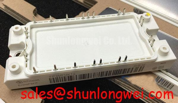
Before applying a DC link, isolate the drive, discharge its energy storage, and use a digital multimeter in diode check mode to screen the main switching paths and the antiparallel diode. This cold test is a practical first filter for a suspected Fuji Electric 6MBI35S-120 in a CNC servo amplifier, robot axis drive, or industrial inverter.
The module is specified for a 1200 V collector emitter voltage, a 35 A continuous collector current at TC = 80°C, and a collector emitter saturation voltage of 2.1 V at 35 A. Its listed maximum power dissipation is 240 W per IGBT, while the operating junction temperature range is −40°C to +150°C. The isolation rating is 2500 V AC for one minute. These are official device specifications and should be separated from the limits imposed by the complete converter, cooling assembly, switching frequency, and protection system.
For the cold inspection, keep the gate terminals electrically separated from the driver board. Probe the relevant collector emitter paths in both polarities, then check the antiparallel diode path with the meter’s diode function. A repeatable forward indication in the expected direction and a blocked reverse indication provide useful screening evidence. An open circuit in both directions, a near short in both directions, or a reading that changes substantially when the leads are repositioned deserves comparison with an unused reference device and a visual inspection of the surrounding circuit.
The gate circuit requires a separate check. Measure gate to emitter leakage with the module unpowered and the driver disconnected, using the test voltage and procedure approved for the service bench. The purpose is to identify an unexpected conductive path rather than to assign a universal pass or fail resistance value. Gate leakage can also be influenced by contamination, moisture, board residue, or a connected driver component, so the module should be isolated before drawing a conclusion.
Inspect the terminal area for heat discoloration, loose hardware, cracked insulation, damaged screw threads, and signs of arcing. Check that the busbar geometry has not forced mechanical stress into the module terminals. In a high dynamics multi axis CNC or robotics servo, the short commutation loop should remain physically compact, with gate and power return paths arranged according to the driver layout. This is a Design Consideration, not a published dimensional guarantee for this particular module.
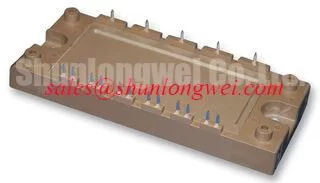
During replacement screening, compare the original circuit topology rather than matching voltage and current labels alone. The related 6MBI75S-120-01 may be reviewed as a separate Fuji Electric module for a different current class, but its electrical, mechanical, and thermal conditions must be checked independently before any substitution decision. A higher current marking does not by itself confirm terminal compatibility, gate-drive compatibility, or equal switching behavior.
Transient Dynamics and Electrical Design: Preventing Spurious Power-Up Shoot-Through on 6MBI35S-120
Keep the high voltage DC link disabled until the auxiliary gate-driver supply, UVLO interlocks, and gate-state feedback are stable. This sequencing is an Engineering Recommendation for preventing an undefined gate condition during startup; the exact negative turn-off bias must be selected by the system designer after reviewing the driver, insulation system, switching speed, and gate-emitter limits.
For the specified commissioning approach, engineers may evaluate an active negative turn-off bias in the −5 V to −15 V range as a driver tuning window, not as an official 6MBI35S-120 rating. The selected value must remain within the gate-drive limits stated for the actual module and driver combination. The driver should hold both complementary switches in a known off state while its supply rises, and the UVLO circuit should prevent a partial gate pulse from reaching the module.
Gate-loop parasitic inductance can convert rapid current change into gate voltage disturbance. Keep the driver return path controlled, minimize the physical loop area, and place the gate damping network according to the power-stage layout. The correct resistor and damping arrangement are system-determined: verify turn-on and turn-off waveforms at the module terminals with suitable high-voltage differential and isolated gate probes. Look for unwanted gate movement during the opposite switch transition, excessive collector emitter overshoot, and ringing that crosses the driver’s effective threshold.
Do not treat a clean static gate measurement as proof of dynamic immunity. A servo amplifier can pass a bench resistance check while still producing shoot-through during power-up, current reversal, or a fault reset. Check the real sequencing path from the controller enable signal through the isolated driver, UVLO logic, gate clamp, and DC-link contactor. The test should include repeated enable and disable cycles with the current command held at zero before progressively applying the intended operating conditions.
The local DC-link support network also affects the transient seen by the module. Where a bootstrap or auxiliary boost arrangement is used in the driver, inspect the charging diode, capacitor condition, return path, and high-frequency charging current. The capacitor must retain sufficient voltage during the gate-drive demand imposed by the switching pattern; its required value and voltage margin are calculated from the driver’s gate charge, quiescent demand, switching duty, ripple allowance, and temperature. These values are not established by the 6MBI35S-120 power ratings alone.
Fast semiconductor fuse coordination belongs to the complete protection design. Compare the fuse clearing I2t with the module’s permitted short-circuit and surge conditions from the applicable device documentation, while accounting for wiring inductance, DC-link capacitance, fuse tolerance, and the fault detection delay. A fuse that interrupts quickly may still permit a damaging energy pulse if the gate driver remains active or if the commutation loop produces a high voltage overshoot before isolation. The protection test should therefore examine gate shutdown timing, fuse interruption behavior, and the measured collector emitter waveform together.
The 2MBI200S-120 can be evaluated as a separate rectifier or front-end association in a broader converter topology. It should not be treated as an automatic electrical match for the inverter stage. The front-end device, DC-link capacitor bank, braking circuit, fuse, contactor, and IGBT module must be assessed as one energy path, particularly when a multi-axis servo cabinet shares a common bus.
For switching principles and gate-loop implementation, engineers can also consult Fuji Electric Discrete IGBT & SiC MOSFETs as a manufacturer technology reference. The page covers broader semiconductor categories and should not be read as a substitute for the specific electrical conditions of this module.
6MBI35S-120 Thermal Electrical Optimization: Preventing Ceramic Substrate Rupture During Practical Tuning
Check the heatsink contact surface and the module baseplate before tightening any replacement. A visible convexity, burr, embedded metal particle, or uneven mounting surface can concentrate mechanical load and reduce the intended thermal contact area. Place a straightedge across the heatsink and inspect the baseplate under clean bench lighting; do not force a warped module flat with the mounting screws.
Use a thin, continuous thermal interface layer applied evenly across the contact zone. A 50 to 80 µm TIM layer is a general Design Consideration for a controlled mounting process, not an official Fuji Electric dimensional specification for this module. The actual result depends on compound viscosity, surface roughness, application method, baseplate condition, and clamping pressure. Excess compound can increase thermal resistance and contaminate nearby insulation, while insufficient coverage leaves air pockets.
Install the fasteners progressively in a diagonal cross pattern so that the baseplate settles against the heatsink without twisting the ceramic substrate. Use the torque specified for the actual screw, washer, thread, and heatsink assembly. If the mechanical design uses M5 hardware, a controlled starting range of 2.5 to 3.5 N·m may be used only as a general industry Design Consideration after confirming the module manufacturer’s mounting instructions and the hardware grade. The confirmed assembly specification takes priority.
⚠️ Field Alert: Never tighten one corner fully before the opposite fasteners are seated, because uneven clamping can damage the substrate or leave a concealed thermal gap.
After tightening, inspect the interface from the accessible edges for displaced compound and confirm that the heatsink has not shifted against the terminal block. Measure the heatsink temperature during a controlled load test and compare it with the electrical behavior of the phase leg. The official 240 W maximum power dissipation per IGBT is a device rating under specified thermal conditions, not a direct prediction of allowable cabinet output power. System losses, switching frequency, airflow, heatsink thermal resistance, ambient temperature, and duty cycle determine the practical operating point.
Keep power terminals, gate wiring, and cooling hardware mechanically independent where possible. Busbar strain should not pull on the module terminals, and the gate harness should not be routed alongside a high-current commutation path without a deliberate return path. Clearance and creepage must be reviewed against the complete working voltage, pollution environment, enclosure construction, and applicable equipment standard. The module’s 2500 V AC one-minute isolation rating is an official isolation specification; it does not independently certify the finished drive or guarantee system-level insulation performance.
When a thermal alarm appears after replacement, record the load profile, heatsink temperature, phase current balance, switching waveform, and mounting condition before removing the module. Uneven heating can arise from electrical imbalance, poor interface contact, gate timing, blocked airflow, or a damaged neighboring component. Compare the three phase legs under the same test conditions instead of assigning the symptom to the IGBT module without measurement.
For a CNC operator panel, robotic servo cabinet, or variable-frequency drive enclosure, the integrator should verify terminal geometry, gate-drive polarity, protection timing, cooling clearance, and insulation coordination against the original equipment documentation. The 6MBI35S-120 ratings provide the device-level electrical reference: 1200 V VCES, 35 A continuous IC at 80°C case temperature, 2.1 V VCE(sat) at 35 A, −40°C to +150°C junction operation, and 2500 V AC isolation for one minute. The final acceptance test remains a function of the complete servo power stage and its measured operating margins.