

Content last revised on October 14, 2026
Benchtop Waveform Tuning: Mitigating Stress via Isolated DC-DC Power Supply Sizing on FP35R12KT4
With the DC link discharged and verified safe, disconnect the gate-driver connections before comparing cold-state resistance across the FP35R12KT4 power terminals against the equipment schematic. Record meter polarity and isolate parallel circuit paths; a low reading through connected circuitry is not enough to condemn the module. Inspect terminal seating, mounting surfaces, and evidence of uneven heatsink contact before reconnecting the driver.
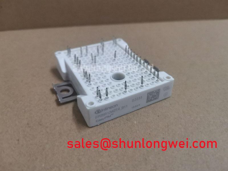
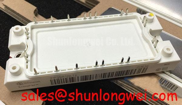
The FP35R12KT4 is an Infineon IGBT module with an official specified voltage rating of 1200 V, rated current of 35 A under the specified datasheet conditions, and Module package classification. These product specifications establish the starting point for identification. Gate-drive compatibility, terminal assignment, thermal operating conditions, and mechanical fit govern whether the unit can be integrated into an existing power assembly.
Capture the isolated gate-supply rails during switching bursts rather than accepting an unloaded DC voltage measurement as proof of adequate driver power. As a Design Consideration, the isolated supply must support gate charging, driver consumption, and transient loading without losing the intended on-state or off-state bias. Rail movement synchronized with switching can help distinguish supply regulation problems from noise entering through the measurement setup.
Size the driver supply from the selected switching frequency, gate-charge operating point, driver losses, and startup behavior. The gate-charge value used for that assessment must correspond to the relevant collector voltage and gate excursion. Average power alone does not describe the local pulse demand: inspect decoupling placement and the current path between the supply, driver output stage, and module terminals. Final component selection belongs to the system design and its measured operating envelope.
Reinforced isolation and common-mode transient immunity are properties of the selected driver and power-supply arrangement, not specifications established here for the FP35R12KT4. As a Design Consideration, evaluate working voltage, insulation classification, barrier capacitance, and transient immunity against the actual application. A withstand-test rating does not independently establish continuous working-voltage suitability, and a driver’s immunity rating does not describe the isolated supply’s behavior.
For driver selection, Infineon EiceDRIVER™ galvanically isolated gate-driver ICs provide manufacturer documentation for comparing isolation and switching-interface requirements. Measure the gate waveform with a suitably rated differential or isolated probe referenced locally to the intended emitter return. Repeat the observation at the driver output to identify whether ringing develops in the interconnect rather than inside the driver circuit.
Where the system employs negative off-state bias, assess its magnitude against the module’s permitted gate-voltage limits and the driver’s supply range. Negative bias can influence resistance to unintended turn-on, but it does not replace a controlled return path or adequate transient immunity. Preserve clearance and creepage across the assembled isolation boundary using the equipment’s applicable insulation requirements; connector contamination and cable routing belong in that assessment alongside PCB spacing.
Field Alert: Never attach an earth-referenced oscilloscope ground clip to a switching emitter node; use a measurement arrangement rated for the node’s voltage and transients.
Field Diagnostics & Commissioning: Evaluating Thermal Capacitance vs Heatsink Performance in FP35R12KT4 Topologies
Record the overload pulse duration, repetition pattern, and case-temperature trend before judging whether the heatsink can support the FP35R12KT4 operating cycle. As a Design Consideration, short pulses and sustained loading create different thermal demands: internal transient heating can precede a noticeable change at the heatsink sensor. A stable external temperature therefore does not establish a safe peak junction temperature during repeated acceleration or braking events.
For an Engineering Calculation using a validated transient thermal model, a rectangular loss pulse can be assessed through the relationship ΔTj(t) = P_loss × ZthJC(t), with the junction-temperature rise referenced to the applicable case temperature. Repeated pulses require thermal-history superposition or time-domain simulation. Multi-RC coefficients must come from the relevant manufacturer model, and their Foster or Cauer representation must be handled correctly rather than joined arbitrarily to an external heatsink network.
Build the loss waveform from the actual conduction and switching conditions instead of substituting the module’s current rating for dissipated power. Compare the calculated peak junction temperature with the permitted operating boundary and account for uncertainty in losses, case measurement, and cooling performance. For commissioning, examine both the first overload pulse and the accumulated temperature after repeated cycles; these observations answer different questions about available thermal margin.
Inspect the thermal interface for incomplete coverage, contamination, or impressions that suggest uneven contact. As an Engineering Recommendation, select the interface material and applied thickness using the module mounting instructions, surface condition, and material supplier’s guidance. Apply mounting force progressively and evenly through the specified fasteners, following the documented sequence and torque rather than importing a generic bolt value. Excess material is not a reliable remedy for a distorted mounting surface.
For compatibility assessment, engineers may evaluate this module for a compact industrial inverter or high-speed CNC spindle drive, subject to circuit and mounting verification. The FS35R12YT3 is a separate comparison candidate, not an established drop-in replacement. Use the following checks before deciding whether either part matches the equipment bill of materials.
| Compatibility check | FP35R12KT4 | FS35R12YT3 |
|---|---|---|
| Manufacturer | Infineon | Consult manufacturer datasheet |
| Voltage rating | 1200 V — Official Specification | Consult manufacturer datasheet |
| Rated current | 35 A under the specified datasheet conditions — Official Specification | Consult manufacturer datasheet and rating conditions |
| Package classification | Module — Official Specification | Compare outline and mounting drawing |
| Replacement decision | Check equipment circuit, terminal map, and drive conditions | Compare topology, terminals, gate characteristics, and thermal limits |
For background on interface heat flow and cooling architectures, The Advanced Thermal Management Revolution offers broader technical context; it does not establish this module’s internal construction. If the surrounding equipment includes bidirectional battery conversion, evaluate its charging and discharging loss profiles separately. Reducing unnecessary temperature excursions is a Design Consideration, not a quantified lifetime claim for this product.
Field Diagnostics & Commissioning: Preventing High-di/dt-Induced Gate-Loop Disturbances in FP35R12KT4 Topologies
Trace the driver’s emitter return to the module terminal drawing before changing gate resistance or off-state bias. As a Design Consideration, voltage developed across shared power-current impedance can disturb the effective gate-to-emitter voltage. Distinguish the load-current route from the control return in the schematic and physical assembly; do not assume that a nearby small terminal is a dedicated Kelvin emitter connection without its documented pin assignment.
Keep the gate-drive outgoing and return paths closely coupled while avoiding unnecessary shared sections with the load-current path. Compare gate voltage at the module with the signal at the driver during turn-on and turn-off. A disturbance correlated with collector-current transitions warrants inspection of return routing, connector contact, and probe placement. It does not, by itself, identify a defective module or prove unintended turn-on.
In the surrounding power architecture, regenerative energy needs a defined destination. Where the equipment uses a braking chopper and resistor, inspect the chopper command, resistor connection, protection state, and DC-link response during deceleration. The resistor’s pulse-energy capability and cooling must match the equipment duty. The separately documented FF500R12KE4 can be reviewed when assessing another switching stage; it should not be treated as a rectifier or a compatible FP35R12KT4 substitute without circuit-level verification.
Also distinguish a discrete module installation from an intelligent power-module assembly. Infineon CIPOS™ Maxi IPM documentation provides a separate reference for integrated drive and protection arrangements, not evidence that those functions are included in this product. During controlled recommissioning, correlate commanded switching, local gate waveforms, and DC-link behavior so that any remaining disturbance can be assigned to the driver path, power interconnect, or energy-handling circuit.