Content last revised on October 19, 2026
Assembly Integrity & Layout Architecture: Implementing PCB Symmetry Considerations for Dual IGBT for 2MBI300P-140-03
I trace each gate-driver return to its emitter connection before assessing PCB symmetry. As a Design Consideration, shared impedance between the gate return and the main emitter current path can introduce unwanted feedback during switching. Route the external driver return separately from high-current conductors wherever the documented terminal arrangement permits. A dedicated internal Kelvin emitter connection must not be assumed from the dual configuration or package designation.
Compare the two gate loops by electrical function rather than visual symmetry alone. Track their outgoing and returning paths, connector transitions, and proximity to the switching node. Unequal coupling can produce different gate waveforms even when the driver components match. Keep clearance around high-voltage conductors consistent with the equipment’s insulation-coordination requirements; PCB spacing belongs to the system design, not to an inferred module-specific rule.
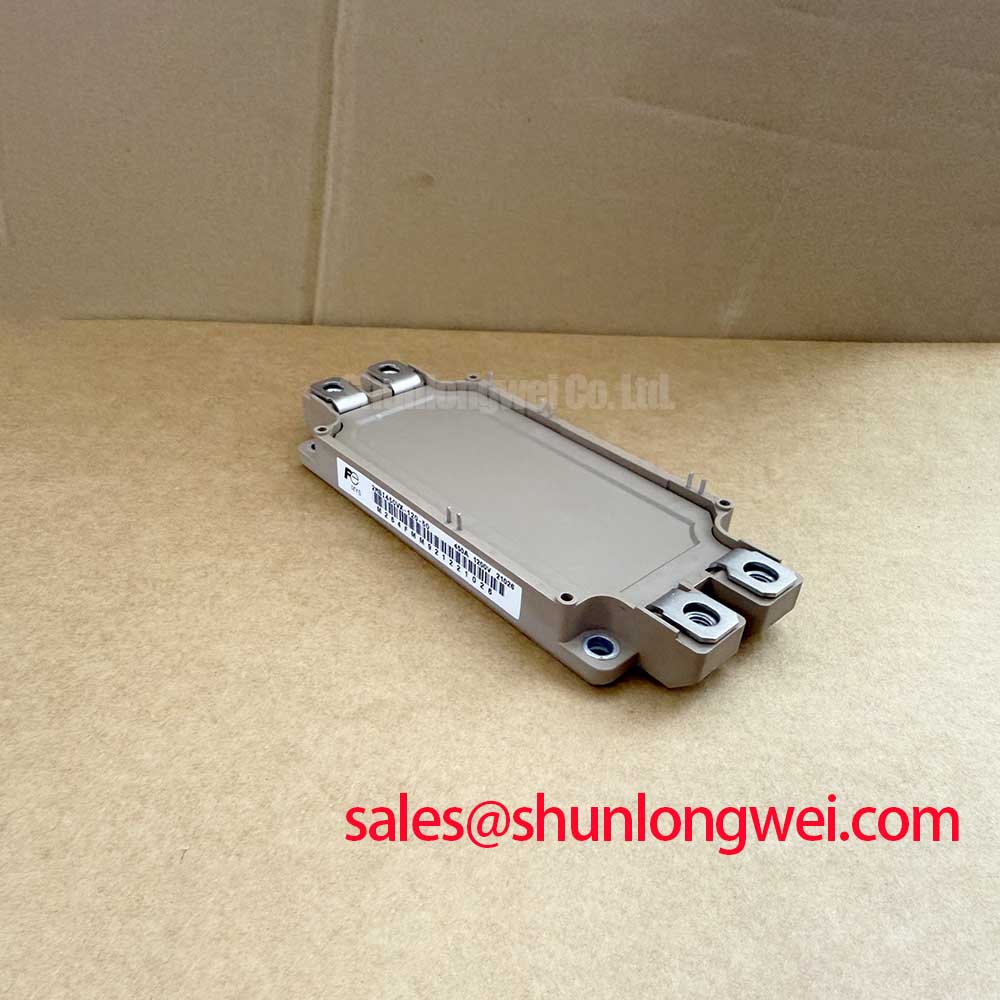
The Fuji Electric 2MBI300P-140-03 has an Official Specification of 2.8 V typical collector-emitter saturation voltage at 300 A. This is a typical conduction characteristic, not a maximum loss guarantee across operating temperatures. Its 1400 V collector-emitter rating and 300 A at a case temperature of 25°C establish separate electrical boundaries; the thermal path and switching conditions determine the usable operating envelope.
Design Consideration: Keep the commutation bus paths compact and electrically balanced to reduce turn-off overshoot, then verify voltage margin with double-pulse measurements under representative system conditions.
For overvoltage protection, distinguish incoming surge suppression from local switching-transient control. An MOV network can participate in the equipment’s surge strategy, but it does not remove the inductance between a local switching loop and its protective components. Evaluate clamp behavior, placement, and coordination with the existing DC-link protection using measured terminal waveforms.
During sourcing comparisons, the 2MBI150NC-060-10 should be treated as a separate Fuji model for specification comparison, not as an established interchangeable replacement. Match electrical ratings, terminal assignments, mounting geometry, driver compatibility, and thermal requirements before assessing any substitution.
2MBI300P-140-03 Operational Boundaries: Pre-Installation Junction Health Check
Disconnect the module from parallel circuit paths and verify that the DC link is discharged before performing diode-mode checks. As a Design Consideration, identify the collector, emitter, and gate connections from the terminal drawing, then record directional readings across each power section. Where the circuit diagram identifies an antiparallel diode, compare its forward and reverse behavior under the same instrument conditions. A meter reading is a screening observation, not a junction qualification result.
Keep the gate at a defined emitter-referenced potential during power-terminal checks so that accumulated charge does not alter the result. Compare both sections and investigate unexpected asymmetry after excluding connected snubbers, driver circuits, and residual charge. Do not assign a universal forward-voltage pass band: test current, temperature, and measurement topology influence the displayed value.
A multimeter can reveal gross gate-to-emitter abnormalities, but it cannot establish specified gate leakage or switching integrity. Leakage assessment requires a controlled, current-limited measurement using the manufacturer’s test conditions. Cold screening also does not establish an allowable operating frequency; frequency selection depends on switching losses, gate-drive behavior, and the cooling arrangement.
Inspect the mating heatsink surface before applying thermal interface material. As an Engineering Recommendation, use the interface supplier’s application method to obtain a continuous, controlled layer without treating a generic thickness as an M239 requirement. Check flatness, cleanliness, and coverage because tightening force cannot compensate reliably for debris or uneven contact.
Bring the mounting fasteners into engagement progressively using a cross-pattern sequence where the mounting arrangement permits. Apply the specified torque for the actual module and fastening hardware rather than adopting a generic bolt-size value. Keep terminal fastening loads separate from base mounting loads, and support busbars so that alignment does not depend on pulling the module terminals into position.
For compatibility assessment in a heavy-duty variable-frequency AC motor drive, compare the existing heatsink, DC-link stress, duty cycle, and gate-driver interface with these module boundaries. In a bidirectional DC-DC battery charge/discharge stage, changing load direction can alter the thermal duty of each switch position. The Peak Efficiency in Solar and Energy Storage guide provides broader topology context; thermal-cycle assessment should remain tied to the actual operating profile rather than an assumed service-life extension.
Field Diagnostics & Commissioning: Common-Mode Transient Immunity in 2MBI300P-140-03 Topologies
Capture the gate-emitter voltage at the module connection while observing the driver command and switching-node transition with appropriately rated measurement equipment. As a Design Consideration, an unintended gate excursion can arise from capacitive coupling, emitter-path impedance, driver behavior, or probe pickup. Correlate timing across these signals before attributing the disturbance to an isolation component.
CMTI belongs to the gate-driver isolation path and its operating conditions, not to the IGBT module’s collector-emitter rating. Check the installed optocoupler or digital isolator documentation, including transient polarity and test conditions. Likewise, an isolation withstand voltage alone does not establish reinforced insulation: barrier classification, working voltage, layout, and equipment requirements must be assessed together.
For Miller-related disturbances, examine the off-state gate return, driver sink behavior, and coupling from nearby power conductors. Evaluate gate damping or clamping changes against both false-turn-on susceptibility and switching loss. Confirm the result across the intended operating conditions instead of selecting a gate-drive voltage or resistance from an unrelated module example.
If the existing driver uses a bootstrap supply, observe its voltage through the relevant switching sequence. Recharge opportunity, capacitor behavior, diode recovery, and driver consumption can affect the available gate drive. Resolve supply droop separately from common-mode interference; similar-looking gate disturbances need not share a cause.
Fuji Electric’s RC-IGBT module information and discrete IGBT and SiC MOSFET resources provide manufacturer context for distinct semiconductor families, not evidence that their structures or drive requirements apply to this model. During commissioning, retain synchronized gate, driver-supply, and collector-emitter traces so that each protection or layout change can be evaluated against the same observed disturbance.