



Content last revised on September 30, 2026
Assembly Integrity and Layout Architecture for 2MBI400TC-060
| Manufacturer | Fuji Electric |
|---|---|
| Product Category | IGBT Module |
| Model | 2MBI400TC-060 |
| Rated Voltage | 600.0 V |
| Rated Current | 400.0 A |
| Package | Fuji Power Module |
Measure the gate to emitter path with the equipment isolated, then compare the cold state readings of the replacement unit against the known good phase leg before connecting the driver harness. A reading that differs between parallel device positions can indicate a gate loop, terminal contact, or driver interface issue that requires circuit level inspection rather than immediate module replacement.
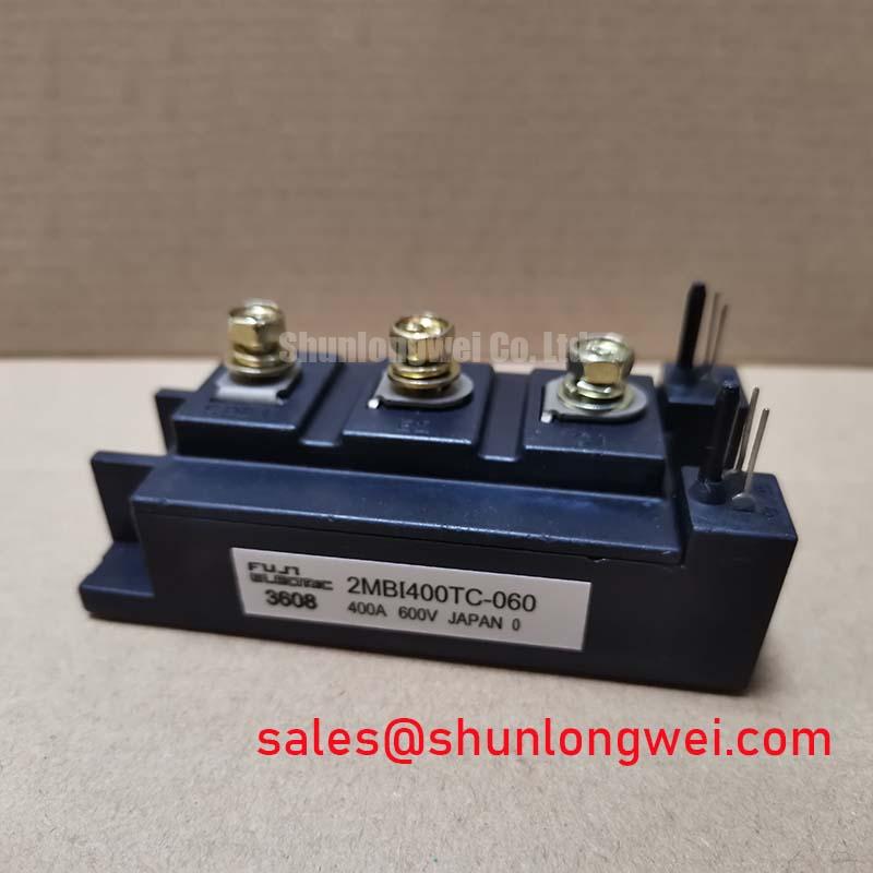
The 2MBI400TC-060 is a Fuji Electric IGBT module rated at 600.0 V and 400.0 A, housed in a Fuji Power Module package. Those ratings identify the device class, but they do not define the allowable switching conditions of a complete converter. When evaluating the module for a multi megawatt offshore or onshore wind turbine full scale converter, the gate driver, DC link, phase leg arrangement, cooling path, and protection coordination must be checked as one switching system.
High common mode transients on an industrial drive board can couple through the isolation barrier and gate driver return path. Designers should verify the isolator or optocoupler data for common mode transient immunity under the actual switching waveform, then inspect the physical routing around the gate, emitter return, and power terminals. Keep the gate drive loop compact, route the return path with the corresponding signal path, and prevent high current commutation conductors from sharing impedance with the gate reference.
A Miller clamp can be considered when the driver architecture supports it and when measured collector voltage transitions create an unwanted gate voltage excursion. A negative gate bias may also be evaluated by the system designer, but its value, timing, driver compatibility, and insulation coordination are system determined. The original driver documentation must be checked before applying any negative bias because the module rating alone does not establish a permitted gate voltage range.
For high voltage converter assemblies, clearance and creepage around the main terminals should be evaluated against the working voltage, pollution environment, insulation system, and applicable equipment standard. Do not infer an insulation rating from the 600.0 V collector emitter rating. The replacement assembly should be inspected for correct terminal orientation, flat mounting, clean contact surfaces, and secure mechanical retention before low voltage gate testing.
Field Alert: Disconnect the DC link and gate driver supply before removing or inserting the module, and follow the original assembly hardware specification for mounting pressure and thermal interface preparation.
2MBI400TC-060 Circuit Protection and Reliability
Capture the gate signal, collector emitter voltage, and phase current during a controlled switching test whenever the converter reports an overcurrent or short circuit event; the timing relationship between these waveforms is more useful than treating the protection alarm as proof of a failed IGBT.
A short circuit protection scheme for a high power IGBT stage normally combines desaturation or overcurrent detection with a controlled gate turn off sequence. The protection threshold, blanking interval, fault latch behavior, and soft turn off profile must be matched to the driver and the complete power loop. The available model rating does not by itself verify a particular short circuit safe operating interval, so the system engineer should use the applicable Fuji documentation and measured test results when setting protection behavior.
Two stage soft turn off can be evaluated where rapid gate removal produces excessive inductive voltage overshoot. The first controlled reduction limits the immediate current transition, while the following gate discharge completes the shutdown after the driver has confirmed the fault condition. The actual timing and gate resistance remain dependent on stray inductance, DC link voltage, load current, gate charge, driver capability, and protection response.
In regenerative braking applications, the chopper path must be examined together with the braking resistor, DC link capacitor bank, current sensor, and thermal monitoring. The module can be evaluated in a braking chopper position, but resistor energy absorption, duty cycle, cooling, and fault isolation are properties of the assembled system. Fuji Electric provides background information on Fuji Electric Brake Chopper IGBT Modules that can help engineers compare the functional role of chopper devices during topology review.
Line frequency ripple from a wind turbine converter or bidirectional DC to DC battery interface can create repeated thermal loading in the switching stage. Designers should review junction temperature movement, case temperature measurement location, switching losses, conduction losses, and cooling plate behavior over the complete charge and discharge cycle. A single steady state temperature measurement does not establish thermal cycle life.
RC snubber networks may reduce ringing when the measured waveform shows a repeatable high frequency transient associated with the commutation loop. Snubber capacitance, resistance, pulse energy, physical placement, and voltage rating should be selected from measured waveforms and loss calculations. The snubber must be tested with the actual busbar and module arrangement because moving the measurement probe or changing the loop geometry can materially alter the observed ringing.
2MBI400TC-060 Operational Boundaries and Parallel Current Sharing
Check the current in each parallel phase path with matched probes during both low load and high load operation, then compare the gate to emitter waveforms at the same time reference before adjusting the control system.
The positive temperature coefficient often associated with IGBT conduction voltage can support static current sharing between parallel devices, but it does not guarantee dynamic sharing during turn on or turn off. Differences in gate loop inductance, driver output impedance, emitter return layout, terminal resistance, thermal contact, and signal delay can cause transient imbalance even when the average current appears acceptable.
When multiple modules are considered for a converter leg, use symmetrical power paths and symmetrical gate drive routing. The collector and emitter conductors should have comparable electrical geometry, while the gate return should avoid carrying the high di per dt current of the main commutation loop. A Kelvin emitter connection must not be assumed unless it is explicitly provided by the module terminal arrangement and the original application documentation.
For a wind turbine full scale converter, parallel current sharing should be examined during torque changes, grid disturbances, regeneration, and cooling system transitions. The current sensor locations matter: a sensor that measures only the combined phase current cannot reveal unequal current distribution between individual modules. Engineers should use appropriately located probes or temporary measurement points during commissioning and fault investigation.
Compare the cold resistance and diode conduction path of each installed position with the power isolated. Unequal readings may result from connected snubbers, driver components, current sensors, or other parallel paths, so the measurement should be repeated with the relevant external circuits separated where the service procedure permits. This test provides an initial electrical screen and does not replace an operating waveform assessment.
For a neutral reference during technology comparison, engineers may review 2MBI150NC-060-10 as a separately specified Fuji Electric module. Similar voltage marking does not establish pin compatibility, current equivalence, thermal interchangeability, or control compatibility. Any possible substitution requires a terminal, mechanical, electrical, thermal, and protection review against the original converter design.
Benchtop Waveform Tuning with Planar Busbar Geometry
Place the oscilloscope probe at the module terminals and inspect the turn off collector emitter waveform with the shortest practical measurement loop before changing gate resistance or adding a snubber.
Turn off overshoot is governed by the interaction of DC link voltage, commutation current, switching speed, and stray inductance. The relationship can be used as an engineering calculation to explain why a small change in busbar geometry may produce a large voltage difference, but the acceptable peak must be verified against the module voltage rating, operating margin defined by the system designer, and the actual switching waveform.
A planar laminated busbar arrangement can reduce the loop area between the positive and negative DC conductors when the mechanical assembly allows it. Keep the high current path short, maintain controlled separation between power and gate circuits, and avoid routing the gate return alongside a conductor that carries the main commutation current. The target inductance and busbar dimensions are system design values and should be established by measurement or validated electromagnetic modelling rather than copied as universal limits.
Snubber selection should begin with the measured ringing frequency, voltage excursion, current transition, pulse repetition, and available thermal path. The capacitor must tolerate the repetitive pulse current and voltage stress, while the resistor must absorb the associated transient energy without becoming an unintended hot spot near the gate driver or insulation barrier. A snubber that suppresses one test condition may increase switching loss under another, so validation should cover the complete operating envelope.
Use differential voltage probes with suitable common mode capability, confirm probe compensation, and compare the measured waveform with a second measurement location before drawing a conclusion about device stress. False overshoot can come from probe ground lead inductance, poor probe placement, or an unsuitable reference point. The final design review should correlate the bench waveform with thermal measurements, protection response, and the DC link operating condition.
Engineers assessing converter efficiency and switching topology can also consult the Peak Efficiency in Solar and Energy Storage technical guide for broader inverter architecture context. Fuji Electric’s RC IGBT Modules information may be useful when comparing integrated reverse conducting device concepts, but it does not establish interchangeability with the 2MBI400TC-060.