



Content last revised on September 10, 2026
2MBI600U2E-060 Thermal-Electrical Optimization: Galvanic Gate Drive Isolation, Reinforced Practical Tuning
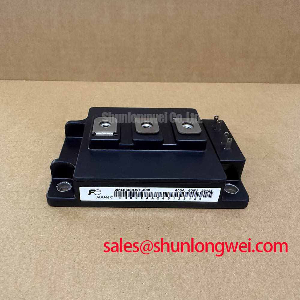
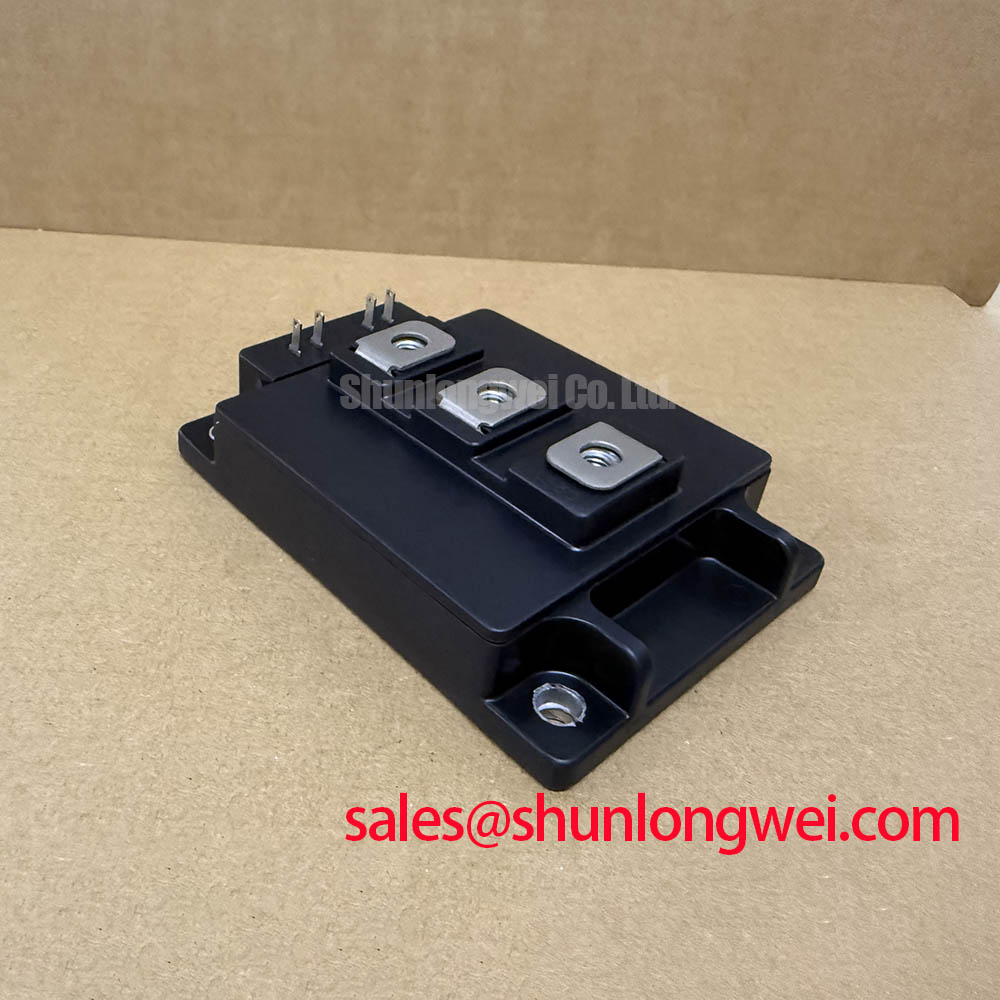
With power removed, verify the nameplate against the replacement record, inspect the module housing and terminals for mechanical damage, then perform cold resistance checks only between terminals identified by the original circuit documentation. The Fuji Electric 2MBI600U2E-060 is an IGBT module with an official rated voltage of 600.0 V, an official rated current of 600.0 A, and a Module package designation.
| Manufacturer | Fuji Electric |
| Part number | 2MBI600U2E-060 |
| Product category | IGBT Module |
| Official rated voltage | 600.0 V |
| Official rated current | 600.0 A |
| Package | Module |
For a replacement in a high-power converter, the first task is not to connect the gate driver. It is to confirm the original terminal assignment, DC-link polarity, switching position, cooling interface, and protection sequence. The official data supplied for this product confirms the voltage, current, and module category, but it does not establish the isolation rating, common-mode transient immunity, gate threshold behavior, gate resistance, or switching energy for every operating condition. Those values must be checked against the applicable Fuji Electric documentation and the converter design record.
In a full-scale wind turbine converter, the gate driver is separated from the power circuit so that control electronics are not directly exposed to the switching node. A reinforced galvanic isolation barrier may be required by the system safety architecture, while the driver’s common-mode transient immunity must be suitable for the actual switching waveform. Treat these as Design Considerations, not as confirmed specifications of the 2MBI600U2E-060. The system engineer should verify isolation test conditions, insulation coordination, creepage, clearance, and transient performance before energizing the converter.
During field troubleshooting, compare the suspected phase leg with a known-good leg. Check whether the isolated driver supply remains stable during turn-on and turn-off, then observe the gate-to-emitter waveform directly at the module terminals with a properly rated differential probe. A distorted gate signal, unexpected pulse, or timing difference may indicate a driver supply problem, excessive common-mode coupling, probe connection error, or layout-related ringing. It should not be assigned to the IGBT alone without checking the complete signal path.
For compatibility evaluation in a renewable-energy converter, confirm the actual switching frequency, DC-link operating range, overload profile, braking duty, and cooling arrangement. The module’s official 600.0 V voltage and 600.0 A current ratings are identity parameters, not automatic permission to operate at those limits continuously. Designers should verify switching and thermal margins using the manufacturer’s rated conditions and the measured application waveform.
2MBI600U2E-060 Thermal-Electrical Optimization: Active Miller Clamp Implementation Practical Tuning
High dv/dt at the switching node can couple into the inactive device gate through capacitance. If the gate driver cannot hold that gate at the intended off-state potential, an unwanted current pulse may appear. In a high-power regenerative braking chopper or wind turbine converter, this can increase switching loss and may contribute to cross-conduction between devices. An active Miller clamp is therefore a system-level control feature to evaluate when the driver and module are used in a fast-switching bridge.
The appropriate clamp architecture depends on the driver topology, gate-loop inductance, emitter reference, switching speed, and required protection timing. Some systems also evaluate a negative gate bias during turn-off. A negative bias such as the range sometimes used in industrial designs must not be treated as a factory requirement for this particular module unless it is stated in the applicable Fuji Electric specification. The final gate voltage, clamp threshold, desaturation response, soft shutdown behavior, and dead time are system-determined values that require bench verification.
When investigating suspected false turn-on, place the probe between the gate and the correct emitter reference rather than between the gate and a distant control ground. Inspect the driver return path, isolation power supply, clamp transistor, and gate resistor network. If the waveform changes substantially when the probe location changes, the measurement loop may be capturing common-mode movement rather than the actual gate-to-emitter voltage.
The freewheeling diode path also requires attention. Reverse-recovery behavior can interact with stray inductance and switching speed, producing voltage ringing and radiated noise. The linked Fuji Electric Brake Chopper IGBT Modules reference provides useful manufacturer context for braking applications, but system designers should still confirm the exact diode and switching characteristics associated with the selected module. Snubber selection, clamp placement, and damping must be validated from measured overshoot and loss rather than copied as universal values.
In a battery bidirectional DC-DC stage, repeated charge and discharge transitions create a thermal cycle that is determined by current profile, modulation, heat-sink impedance, airflow, and control strategy. The 2MBI600U2E-060 may be evaluated in such a topology where its official voltage and current class matches the system study, but thermal-cycle life, power-cycle capability, and reliability projections require source-backed application data. No field failure rate or service-life figure should be inferred from the part number.
2MBI600U2E-060 Circuit Protection & Reliability: Differential Gate-Emitter Loop Routing
At the module, the gate loop should be treated as a high-speed measurement and power path. Keep the outgoing gate connection and its return physically close, minimize the loop area, and route the return to the emitter reference specified by the original circuit. Do not assume that a visually convenient chassis or power-return point is an equivalent gate reference. The correct arrangement depends on the module terminal structure and the driver board.
High current in the main emitter path can create a voltage difference across shared copper and connection inductance. That voltage may be added to the intended gate-to-emitter signal and can produce oscillation, delayed turn-off, or uneven current sharing. Separating the driver return from the main high-current emitter route is a Design Consideration intended to reduce mutual coupling. Whether a separate auxiliary emitter or Kelvin connection is available must be confirmed from the original Fuji Electric terminal drawing; it should never be assumed from the package label alone.
For a stopped converter, inspect terminal washers, busbar contact areas, insulation sheets, and signs of uneven pressure. Check that the replacement module sits flat on the heat-transfer surface and that the busbar does not apply side load to the terminals. The mounting method, fastener specification, thermal interface material, and tightening sequence should follow the equipment service documentation and the module’s mechanical data.
⚠️ Field Alert: Isolate and discharge the DC link before unplugging gate-drive connections, and verify the absence of hazardous voltage with an approved procedure.
Protection testing should proceed with a controlled low-energy setup before full-power operation. Confirm gate-driver undervoltage behavior, overcurrent detection, desaturation or equivalent fault response, interlock timing, and fault reset logic. A failed pulse during this test may originate in the controller, isolation channel, auxiliary supply, protection circuit, or wiring. Use oscilloscope records from the complete phase leg to separate these possibilities.
When evaluating the surrounding topology, the 2MBI300U4H-120-50 can be reviewed as a neutral reference for an associated rectification or complementary power stage. It is not a substitute recommendation for the 2MBI600U2E-060. Voltage class, current waveform, diode behavior, gate-drive requirements, mechanical footprint, and thermal path must all be compared before any system change.
Benchtop Waveform Tuning: Mitigating Stress via DC-Bus Low-Inductance Laminated Busbar Design on 2MBI600U2E-060
Begin waveform tuning with the lowest practical DC-bus energy and a current-limited test arrangement. Measure the collector-emitter waveform at the module terminals, not at a remote capacitor or test point. Turn-off overshoot is influenced by DC-link voltage, commutation current, switching rate, stray inductance, probe technique, diode recovery, and the position of the local DC-link capacitor. The familiar relationship between overshoot and the product of stray inductance and current slew rate is useful as an Engineering Calculation, but measured results must determine the final clamp and busbar design.
A laminated busbar can reduce the loop area between the switching devices and local DC-link capacitance when its geometry is correctly matched to the converter. The target inductance, dielectric arrangement, current capacity, insulation coordination, and mechanical clearances are system design requirements; they are not official package specifications for this module. Designers should verify peak collector-emitter voltage against the permitted operating envelope during switching tests, including regenerative braking events and abnormal shutdown.
Snubber capacitors should be positioned according to the actual commutation loop and selected from measured ringing frequency, energy dissipation, pulse current, and temperature rise. Increasing capacitance without checking switching loss can move stress from voltage overshoot into the IGBT and capacitor. A practical bench sequence is to record the initial waveform, change one damping element at a time, repeat the measurement at the relevant current, and compare both voltage peak and switching temperature.
For a wind turbine full-scale converter, braking-resistor operation can impose short, high-energy pulses on the chopper stage during DC-link regulation. The control system should be checked for the complete path from overvoltage detection to gate command, chopper conduction, resistor thermal response, and fault shutdown. The module’s 600.0 V and 600.0 A official ratings do not define the resistor value, pulse duration, duty cycle, or cooling requirement. Those conditions are established by the converter manufacturer and verified through thermal and electrical testing.
During final validation, record gate voltage, collector-emitter voltage, phase current, DC-link voltage, heat-sink temperature, and fault signals on the same time base. Check the waveform at cold start and after the converter reaches its normal thermal condition. The Precision Gate Drive Design resource can be used as a related technical reference when reviewing gate-loop behavior and switching-test practice. For comparison with alternative device families, consult Fuji Electric’s High-Speed Discrete IGBTs information while keeping package, isolation, current path, and cooling compatibility under separate review.