Content last revised on October 15, 2026
5SNA0400J650100 Operational Boundaries: Preventing High di/dt Gate-Loop-Induced Transients
High di/dt switching makes the gate return path part of the switching circuit, so the main load emitter reference must be kept distinct from any auxiliary or Kelvin emitter return identified by the applicable terminal drawing. A shared high-current emitter path can develop a transient voltage that appears at the driver reference. The resulting ground movement may change the apparent gate to emitter voltage and contribute to unwanted turn-on, uneven switching, or protection trips.
During commissioning, trace the gate driver output, gate resistor, emitter return, and module terminals as a complete loop rather than checking signal continuity alone. The driver return should follow the intended low-inductance reference directly to the auxiliary return point where that connection is provided. Keep power commutation conductors physically separate from the sensitive gate loop, and avoid routing the gate signal alongside the collector or emitter busbar over unnecessary distance.
For a replacement assessment, compare the installed terminal arrangement, driver polarity, gate clamp network, and interlock sequence with the original PCS design. A compatible voltage and current rating does not by itself confirm gate-loop compatibility. Oscilloscope measurements should be taken at the module-side gate and emitter reference during controlled switching, with probe connections arranged to avoid adding a long measurement loop.
Pro Tip: Use a symmetrical gate-driver return arrangement and verify the resulting gate waveform during turn-on and turn-off testing before applying full converter power.
5SNA0400J650100 Thermal-Electrical Optimization: Symmetrical Busbar Geometry for High-Current Practical Tuning
Symmetrical busbar geometry supports more even current distribution across parallel paths and reduces the imbalance created by unequal stray inductance. In a high-current PCS, the positive and negative DC conductors should form a compact commutation path, while gate wiring remains physically consistent between switching positions. The mechanical layout should also allow the cooling interface to remain flat and fully supported across the module base.
The positive temperature coefficient of VCE(sat) can support steadier static current sharing when parallel semiconductor paths are correctly matched and thermally coupled. This effect does not automatically equalize dynamic switching behavior. Gate loop length, driver output impedance, common emitter inductance, and timing differences still require inspection. Gate resistance should be selected as an engineering tuning variable: lower impedance can increase switching speed and ringing, while higher impedance can reduce edge speed and increase switching loss. The final value should come from measured gate and collector-emitter waveforms.
Thermal installation deserves the same attention as electrical symmetry. Clean the mating surfaces, apply the thermal interface material evenly, and tighten the mounting hardware in the sequence and torque specified by the applicable mechanical documentation. Uneven pressure can create local thermal resistance and mechanical stress, even when the electrical connections appear correct. Cooling flow, baseplate temperature, switching frequency, and battery charge-discharge cycling should be considered together when reviewing thermal behavior.
When the PCS topology permits comparison with another high-power module, engineers may review the neutral product page for 5SLG 0600P450300. Any substitution requires an independent check of electrical ratings, terminal arrangement, gate-drive requirements, thermal interface, and protection coordination.
Field Diagnostics and Commissioning: High-Frequency Commutation Loop Inductance in 5SNA0400J650100 Topologies
Turn-off overshoot is governed by the interaction of commutation-loop inductance, current slew rate, and the DC-link condition. In practical terms, the transient peak rises when the switching loop is physically large or the current changes rapidly. The first commissioning task is therefore to inspect the laminated or closely coupled busbar path from the module terminals to the local DC-link capacitor, rather than attempting to correct every overshoot problem with a gate resistor.
Use a controlled low-energy switching test to compare the collector-emitter waveform at the module terminals with the DC-link voltage. Check probe bandwidth, probe grounding, and measurement placement before interpreting the waveform. A ringing pattern that changes when the probe position changes may be a measurement artifact or a symptom of excessive loop area. Snubber capacitors, damping components, and local overvoltage devices should be evaluated as a coordinated network, with values selected from measured energy, switching frequency, and thermal loss.
Busbar insulation must maintain the required clearance and creepage for the actual working voltage, pollution environment, altitude, and enclosure arrangement. Do not treat a compact busbar as sufficient evidence of insulation adequacy. The same inspection should include sharp conductor edges, unsupported heavy copper, terminal clamping, and the distance between high-voltage nodes and the gate-driver circuitry.
For engineers reviewing high-speed switching behavior and wide-bandgap alternatives, the Wide Bandgap Revolution reference provides additional technology context. It should be used as a design reference rather than as a substitute for measurements on the ABB module and the target PCS.
Transient Dynamics and Electrical Design: Semiconductor Fuse I2t Coordination for 5SNA0400J650100
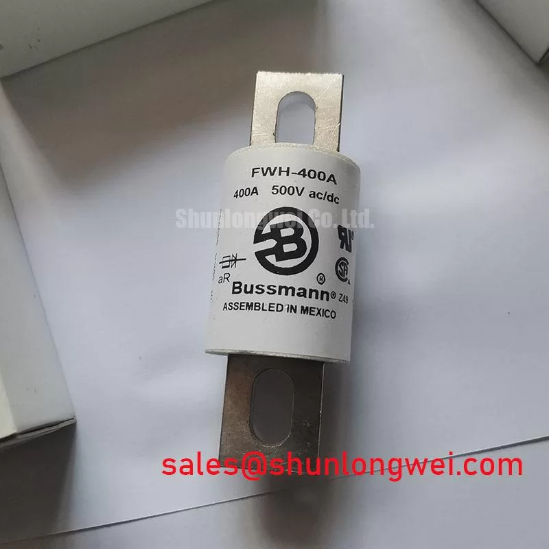
Protection coordination must compare the semiconductor fuse clearing behavior with the module’s specified short-circuit and transient withstand information. The relevant fuse assessment includes total clearing I2t, prospective fault current, DC-link voltage, circuit impedance, and interruption time. A fuse selected only by its continuous current rating may not provide the required sub-cycle protection for an IGBT power stage.
In a centralized battery PCS, the battery rack, DC contactors, pre-charge circuit, capacitor bank, busbar, and inverter bridge all influence the fault energy available to the module. Validate the complete interruption path under the operating conditions defined by the system safety design. The fuse should interrupt the fault without producing unacceptable voltage stress, mechanical force, or enclosure damage. MOVs and other overvoltage absorption components may assist the protection network, but their clamping behavior, energy rating, thermal recovery, and coordination with the DC-link design must be assessed as a system.
After a protection event, inspect the gate-emitter path, collector-emitter isolation, terminal condition, busbar supports, fuse indicators, and snubber components before re-energizing the converter. A protection device that has opened does not identify the initiating mechanism by itself. Review the fault recorder, gate command timing, DC-link waveform, and temperature trend to separate an external short circuit from a switching, cooling, or control problem.
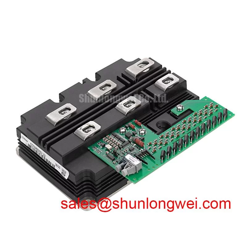
For procurement and maintenance teams, the 6500.0 V voltage specification, 400.0 A current specification, and HiPak Power Module package provide the initial identity check for the ABB 5SNA0400J650100. Final acceptance should include terminal compatibility, mechanical fit, cooling arrangement, gate-drive behavior, and protection coordination within the intended PCS.