Content last revised on September 10, 2026
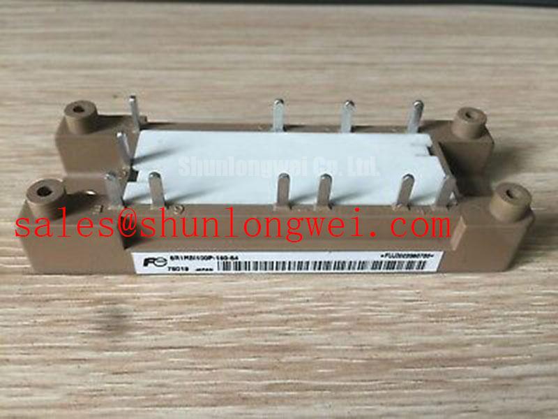
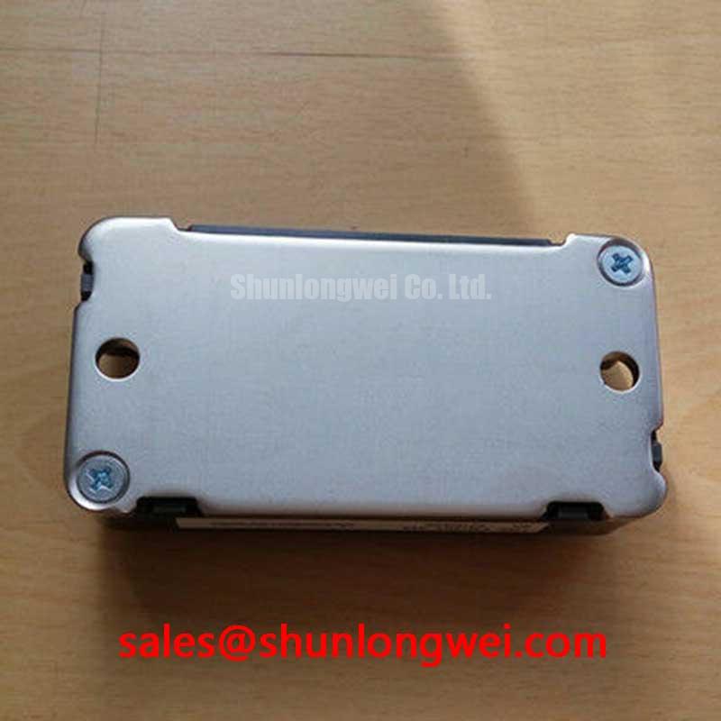
Incoming QA Bench Analysis: Fuji Electric 6MBI100UC-120 6-Pack IGBT Module
When unpacking the Fuji Electric 6MBI100UC-120 on the receiving inspection bench, incoming qualification requires immediate parametric verification prior to chassis integration. As a standard three-phase bridge (sixpack) topology with an integrated current-sensing shunt, this module serves demanding industrial inverter welders and medium-frequency induction heating power supplies. Establishing cold-state baseline measurements allows technicians to verify internal die integrity, junction isolation, and gate threshold uniformity before subjecting the package to high-voltage bus potentials.
| Parameter Symbol | Specification Description | Official Datasheet Value | Data Classification |
|---|---|---|---|
| VCES | Collector-Emitter Voltage Rating | 1200 V | Official Datasheet Specification |
| VGES | Gate-Emitter Voltage Rating | ±20 V | Official Datasheet Specification |
| IC | Continuous Collector Current (TC = 80°C) | 100 A | Official Datasheet Specification |
| IC pulse | Pulsed Collector Current (1 ms) | 300 A | Official Datasheet Specification |
| PC | Maximum Collector Power Dissipation (Per IGBT) | 520 W | Official Datasheet Specification |
| VCE(sat) | Collector-Emitter Saturation Voltage (Chip Typ., 100A, 25°C) | 1.75 V | Official Datasheet Specification |
| Rshunt | Integrated Shunt Resistance Value | 1.5 mΩ | Official Datasheet Specification |
| Rth(j-c) | Thermal Resistance, Junction-to-Case (IGBT Max) | 0.24 °C/W | Official Datasheet Specification |
| Viso | Isolation Voltage (Terminal to Baseplate, AC 1 min) | 2500 VAC | Official Datasheet Specification |
| Tj | Maximum Operating Junction Temperature | 150 °C | Official Datasheet Specification |
💡 Bench Tip: Before conducting digital multimeter checks, ensure complete ESD grounding across your test fixtures. To verify the integrated freewheeling diodes on the 6MBI100UC-120, place your meter in diode check mode with the positive probe on the respective Emitter (or AC phase terminal) and the negative probe on the Collector (DC positive rail). A healthy diode exhibits a cold-state forward drop between 0.38 V and 0.52 V at room temperature (Bench Test Reference at 25°C). Any reading below 0.1 V indicates a shorted internal die, whereas an open loop indicates bond wire lift-off. Additionally, use a micro-ohmmeter across the integrated current shunt terminals to confirm the 1.5 mΩ resistance baseline (Official Datasheet Specification) before mounting the module onto the busbar assembly.
High dv/dt Cross-Conduction Shoot-Through Mitigation via Dedicated Miller Clamps
In medium-frequency induction heating and fast-switching inverter welders, output stages operate under aggressive voltage slew rates often exceeding 10 kV/μs. In a half-bridge branch of the 6MBI100UC-120, when the upper IGBT turns on rapidly, the collector-emitter voltage across the lower IGBT transitions from near-zero to the full DC bus voltage (up to 800V–900V operational levels). This rapid displacement current flows through the lower switch's internal gate-collector parasitic capacitance (Miller capacitance, Cgc). Without adequate suppression, this displacement current generates a voltage drop across the turn-off gate resistor, elevating the gate potential above the threshold voltage and inducing severe shoot-through cross-conduction.
To eliminate shoot-through risks, circuit designers implement active Miller clamping circuits combined with asymmetric gate drive networks. Instead of relying purely on high negative bias supplies, an active Miller clamp driver monitors the gate voltage during the turn-off phase. Once the gate drops below a designated threshold (such as 2.0V relative to the emitter), an internal low-impedance MOSFET shorts the gate directly to the negative supply rail or emitter ground. This creates a low-resistance path that shunts parasitic Miller currents safely away from the gate pin.
A standard industrial recommendation utilizes a negative turn-off bias between -5V and -15V (Typical Starting Point for robust industrial gating). If cost or board real estate mandates a unipolar 0V/+15V drive, an active Miller clamp with a clamp impedance of less than 1.0 Ω becomes mandatory. Keep gate-emitter traces tightly coupled as twisted pairs or closely routed differential PCB layers, maintaining loop areas below 1.5 cm² to prevent magnetic field pickup from high-current welder arc transients.
Symmetrical Busbar Geometry for High-Current Parallel Module Arrays
When induction heating processes demand output levels exceeding the 100A continuous rating of a single 6MBI100UC-120, systems commonly implement parallel inverter legs. Static current sharing among parallel IGBTs is largely governed by the Collector-Emitter Saturation Voltage VCE(sat). The 6MBI100UC-120 features a typical VCE(sat) of 1.75 V (Official Datasheet Specification) at 25°C, possessing a positive temperature coefficient at elevated current levels. As one module carries more steady-state current, its junction temperature rises, increasing its internal on-state resistance and naturally shifting excess current toward the cooler parallel module.
Dynamic current balance during the switching interval, however, is entirely dictated by stray parasitic inductances within the power busbar and gate drive connections. Mismatches as small as 5 nH in loop inductance can force one module to absorb up to 70% of total turn-off energy during switching transitions, leading to localized thermal overstress.
⚠️ Field Alert: Planar, laminated busbar geometry is critical when combining modules. Paralleled modules must share identical path lengths for positive, negative, and AC output phases. Never daisy-chain gate driver signals across parallel modules; each gate must feature an isolated series resistor and matched trace lengths to ensure simultaneous switching. For system overhauls requiring higher continuous current handling without the layout complexity of paralleling multiple devices, evaluating a higher-rated package like the 6MBI300U-120 provides a single-module direct alternative offering 300A capacity within a unified mechanical footprint.
Baseplate Thermal Grease (TIM) Layer Control & Heatsink Mounting Torque Optimization
Managing heat transfer across the copper baseplate is vital to keeping junction temperatures well below the 150°C maximum rating (Official Datasheet Specification) under cyclic welding loads. With a maximum rated power dissipation of 520 W per IGBT device and a low thermal resistance of Rth(j-c) = 0.24 °C/W (Official Datasheet Specification), the junction-to-case thermal path is highly efficient. The primary thermal bottleneck occurs at the case-to-heatsink interface.
Proper application of Thermal Interface Material (TIM) requires controlled layer thickness and verified surface flatness:
- Heatsink Flatness & Roughness: The mounting surface must maintain a flatness tolerance of ≤ 50 μm over a 100 mm span, with a surface roughness Rz of ≤ 10 μm (General Industry Design Consideration).
- Grease Application: Apply a uniform thermal grease layer between 50 μm and 100 μm using a precision squeegee or screen-printing stencil. Excessive thermal grease acts as a thermal insulator, increasing Rth(c-s) significantly.
- Fastening Sequence: Secure module mounting screws using a two-step cross-pattern tightening method. Initially torque all M5 screws to 1.0 N·m (Preliminary Torque), then tighten sequentially to a final torque of 2.5 to 3.5 N·m (Design Consideration for M5 baseplate mounting).
During extended maintenance cycles, baseplate bowing or uneven torque distribution often leads to localized hot spots and solder fatigue under the IGBT silicon chips. For detailed testing procedures on transient thermal impedance curves and root-cause failure analysis in field environments, consult the Field Engineer’s Handbook. High-voltage power topologies across modern equipment platforms also reference design advances established in Fuji Electric 7th-Gen X-Series IGBT Modules to minimize dynamic thermal-mechanical stress.
Galvanic Gate Drive Isolation, Reinforced Creepage & High-CMTI Signaling
Industrial induction heating generators create extreme electromagnetic noise environments characterized by steep voltage and current gradients. The galvanic isolation barrier between the low-voltage control electronics (microcontroller/DSP PWM outputs) and the high-voltage floating half-bridge gates must withstand both high steady-state voltages and massive transient noise. The 6MBI100UC-120 provides an internal terminal-to-baseplate isolation rating of 2500 VAC for 1 minute (Official Datasheet Specification), but external control circuitry must match this insulation integrity.
Optocouplers or digital capacitive/magnetic gate driver ICs chosen for this module should feature reinforced isolation barriers and a Common-Mode Transient Immunity (CMTI) rating of ≥ 100 kV/μs (Design Consideration for heavy industrial switching). When high dv/dt events occur across the half-bridge output, low-CMTI isolators suffer from output state corruption, falsely triggering the gate driver and causing catastrophic branch short-circuits.
Isolated gate driver auxiliary power supplies must minimize input-to-output coupling capacitance (Ciso < 1.0 pF per channel). In high-frequency induction power units, parasitic inter-winding capacitance in DC-DC converters acts as a bridge for common-mode currents, injecting noise directly into digital signal grounds. Maintaining strict PCB creepage and clearance distances (minimum 8 mm for 1200V operational systems under Pollution Degree 2) prevents surface tracking across isolation boundaries. For systems transitioning toward hybrid or higher frequency resonant stages, evaluating wide-bandgap architectures detailed in Fuji Electric Discrete IGBT & SiC MOSFETs provides technical baseline references for gate insulation and parasitic ringing suppression.