
Content last revised on October 26, 2026
Assembly Integrity and Layout Architecture: Implementing Heatsink Surface Flatness and Thermal Grease for 6R1MBI125LP-160-54
- Confirm the cold state terminal polarity and compare diode mode readings across the documented power paths.
- Inspect the copper baseplate, heatsink contact surface, mounting holes, and visible package condition before applying power.
- Verify the gate driver isolation path and DC link discharge condition before connecting the module.
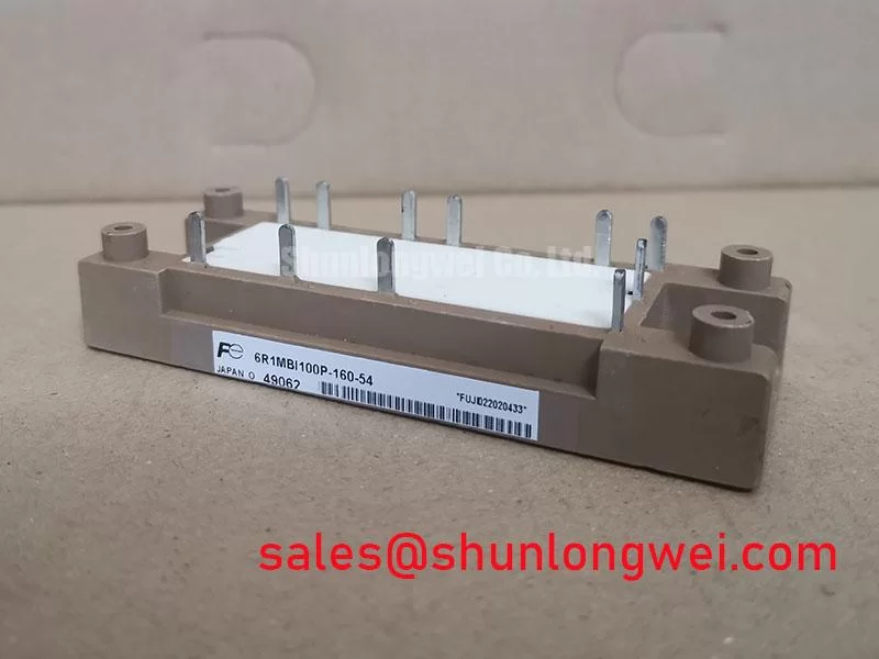
- Record the nameplate rating of 1600.0 V, 125.0 A, and the Fuji Power Module package against the equipment replacement record.
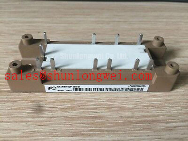
The 6R1MBI125LP-160-54 is a Fuji Electric IGBT module specified at 1600.0 V and 125.0 A, with a Fuji Power Module package. For incoming inspection, treat those three values as official product identification data. Switching behavior, thermal limits, gate charge, isolation test conditions, diode recovery characteristics, and short circuit withstand parameters should be taken from the applicable Fuji Electric documentation used by the equipment owner.
Its voltage and current class makes it a candidate for evaluation in high voltage conversion assemblies such as commercial string inverters, industrial energy storage converters, and micro grid power conversion cabinets. Compatibility remains a system engineering task. The engineer should compare the original module’s electrical topology, terminal arrangement, gate driver requirements, cooling interface, protection timing, and mechanical envelope before authorizing a replacement.
Fuji Electric provides broader reference material through its Power Semiconductor and IPM Modules resource. That material can help engineers interpret the manufacturer’s terminology, while the equipment specific design must remain tied to the correct module documentation and converter schematic.
Start the mechanical inspection with the contact interface rather than the electrical circuit. Place the module and heatsink on a clean bench, remove old thermal interface material, and use a straight edge or approved surface inspection method to identify contamination, local dents, burrs, or visible distortion. The copper baseplate and heatsink must meet the equipment manufacturer’s flatness and surface finish requirements; a visually smooth surface alone does not prove uniform contact.
Thermal interface material should be applied as a controlled, even film across the approved contact area. A practical assembly target may be a thin distribution in the region of 50 to 80 μm, but this is a general engineering consideration rather than a confirmed Fuji Electric production specification for this model. The final thickness depends on the selected compound, surface texture, mounting pressure, and the module maker’s assembly instructions. Excess compound can reduce thermal performance and migrate toward nearby insulation surfaces.
Use a diagonal cross pattern when tightening the mounting hardware so that the baseplate settles progressively instead of being pulled down at one corner. The applicable torque, screw type, washer arrangement, and tightening sequence must come from the module documentation or the equipment service procedure. Keep the power busbar path short and mechanically supported, while maintaining the clearance and creepage distances required by the converter’s working voltage and pollution environment.
When a repaired inverter shows uneven thermal behavior, inspect the imprint of the thermal compound after controlled disassembly. A narrow contact band, a dry region, or compound displaced toward one edge can indicate surface mismatch, mounting sequence problems, or baseplate distortion. Do not use a high torque setting to compensate for a poor heatsink surface. That approach can stress the package and alter the contact pattern.
💡 Bench Tip: Protect the module from ESD during handling, and compare every cold state diode reading with a known good reference taken using the same meter leads, polarity, and temperature.
Assembly Integrity and Layout Architecture: Implementing Bi Directional DC DC Buck Boost Conversion for 6R1MBI125LP-160-54
In a bi directional battery converter, the switching leg must carry energy in both directions as the control system moves power between the battery rack and the inverter link. The 1600.0 V voltage rating and 125.0 A current rating identify the product class, but they do not by themselves define the allowable operating point of a complete buck boost stage. The system designer must correlate switching frequency, modulation range, cooling capacity, bus voltage, current ripple, and protection response.
Gate drive power integrity deserves particular attention on the high side. A bootstrap supply must replenish its capacitor during the available refresh interval while supporting gate charge demand, driver quiescent current, leakage, switching frequency, and the selected gate voltage. The capacitance should therefore be calculated from the applicable gate charge and driver current data, with transient and temperature behavior included in the design review. Do not substitute a generic capacitor value when the relevant Fuji Electric gate charge and driver conditions are available.
For a battery energy storage converter, examine the transition between charge and discharge commands under the actual control sequence. The four quadrant power flow can produce repeated thermal cycling when peak shaving causes frequent high current changes. Thermal monitoring should be correlated with phase current, switching command, heatsink temperature, and fault history rather than judged from a single surface temperature reading.
Keep the gate loop compact and route the power commutation loop separately from sensitive control wiring. Minimize parasitic inductance to reduce gate voltage disturbance and turn off overshoot, then verify the resulting gate emitter waveform at the module terminals with suitable differential measurement equipment. The final loop geometry and gate resistance are system determined. They should be validated during switching tests against the converter’s measured voltage and current margins.
When replacing a module in an existing converter, compare the original gate driver interface, emitter reference, auxiliary terminals, and mechanical position before considering another part. The 1MBI400L-060 is a separate Fuji Electric module that may appear in cross family evaluations, but its rating, topology, pin arrangement, and switching behavior must be checked independently rather than treated as a direct substitute.
6R1MBI125LP-160-54 Circuit Protection and Reliability: Calibrating Short Circuit Energy Let Through Matching
Protection coordination begins with the complete fault current path: DC link capacitance, busbar inductance, semiconductor conduction path, fuse characteristics, gate driver response, and the equipment interruption device. Selective coordination between a high speed semiconductor fuse and the module requires the fuse’s total clearing energy data to be compared with the module’s documented short circuit and transient withstand conditions. The comparison belongs to the complete protection study, not to the module rating alone.
During a service investigation, inspect the fuse holder, bus connections, gate driver fault output, desaturation or overcurrent sensing path, and the DC link discharge circuit as one protection chain. A module that has experienced a short circuit may show altered diode readings, gate leakage, terminal damage, or isolation degradation. These findings should be recorded without assigning a single cause until the driver waveform, fault timing, fuse event, and mechanical condition have been reviewed together.
Gate turn off must be controlled so that the fault current is interrupted without creating an excessive collector emitter voltage excursion. The protection circuit should use the manufacturer’s permitted short circuit conditions, blanking interval, soft turn off behavior, and gate clamp requirements where documented. Any active clamp or Miller control network should be verified at the actual module terminals because PCB level measurements can miss local inductive voltage differences.
Minimize stray inductance in the high current commutation path and place protection sensing where it reflects the module’s real electrical stress. During commissioning, capture collector emitter voltage, gate emitter voltage, phase current, and fault timing with probes suitable for the switching environment. The measured peak and energy should then be compared with the applicable Fuji Electric ratings and the fuse manufacturer’s clearing data.
For a commercial string inverter or micro grid storage converter, coordinate the semiconductor protection with the upstream battery isolation strategy. A fast fuse does not replace gate driver fault handling, and a driver shutdown does not guarantee that stored DC link energy has been removed. The service procedure should identify the discharge confirmation point before any terminal is touched.
Negative off bias can be evaluated as part of a gate control strategy when the driver and module documentation support it. The design principles are discussed in Evolution of Negative Off Bias Gate Drive Circuits. The actual gate voltage, clamp arrangement, and switching timing remain determined by the approved driver design and validated measurements.
6R1MBI125LP-160-54 Operational Boundaries: Evaluating Screening Substrate Ceramic DBC Micro Crack Limits
Isolation screening should be performed with the module disconnected from the gate driver, control board, battery, and DC link. Inspect the terminals, baseplate, mounting region, and insulating surfaces for contamination, tracking, mechanical damage, or visible cracking before connecting an insulation tester. The requested screening reference of at least 500 MΩ at 2.5 kV DC should be treated as an inspection criterion for the applicable service or quality procedure, not automatically as an official production specification for this model unless it appears in the governing Fuji Electric document.
Apply the test between the power terminal network and the baseplate using the approved connection arrangement, test duration, discharge method, and safety controls. A high resistance result is meaningful only when the module is clean, dry, isolated from external circuitry, and tested with an instrument suitable for the voltage level. Surface dust and conductive residue can create leakage paths that do not represent a permanent internal defect, while a stable low result after cleaning requires escalation through the equipment quality process.
Thermal cycling and mounting stress can affect the condition of the ceramic substrate and bonded interfaces in power modules. For that reason, compare the isolation result with the visual inspection, prior service records, and thermal history. Do not press probes against delicate terminal surfaces or use the insulation tester across semiconductor junctions in a way that exceeds the approved test arrangement.
Creepage and clearance must be preserved around the installed module, busbars, fuse connections, and mounting hardware. Industrial airborne dust, moisture, and residue can reduce surface insulation performance, so the enclosure sealing, cleaning method, and pollution control strategy should be reviewed with the converter designer. The module itself should not be treated as an independent EMC, safety, or insulation certification for the complete inverter.
For field replacement, record the cold isolation value, terminal condition, mounting surface condition, and the exact test configuration before energizing the equipment. This creates a useful baseline for later maintenance without assigning unsupported lifetime, FIT, cosmic ray, altitude, or short circuit probability figures to the device.