
Content last revised on September 10, 2026
BSM75GB170DN2 Installation and Rating Overview
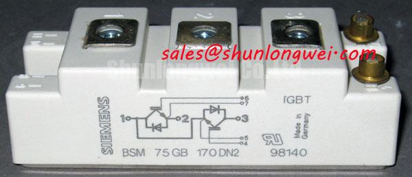
With the converter fully isolated and discharged, first compare the installed module marking and terminal arrangement with the equipment documentation, then inspect the power connections, gate wiring, heatsink interface, and surrounding bus structure before fitting the BSM75GB170DN2. This Infineon power semiconductor is specified as an IGBT Module with an official rated voltage of 1700.0 V and rated current of 75.0 A. These are the confirmed product identity values for this module; switching conditions, gate drive requirements, thermal impedance curves, isolation ratings, terminal assignments, and mechanical mounting details must be verified against the original module documentation and the host equipment design.
| Product attribute | Confirmed value | Classification |
|---|---|---|
| Part number | BSM75GB170DN2 | Official product identification |
| Manufacturer | Infineon | Official product identification |
| Voltage rating | 1700.0 V | Official Specification |
| Current rating | 75.0 A | Official Specification |
| Package | Module | Official Specification |
The voltage and current ratings identify an electrical operating boundary rather than a complete inverter design rule. In a utility scale central photovoltaic inverter, the module selection review should include the actual DC link, expected regenerative events, switching overshoot, cooling conditions, gate driver behavior, protective shutdown sequence, and the original power-stage topology. The 1700.0 V rating is especially relevant when assessing high-voltage conversion stages, but it does not by itself validate suitability in a particular 1500 V photovoltaic inverter.
BSM75GB170DN2 Thermal-Electrical Optimization: Transient Thermal Impedance Practical Tuning
Start thermal evaluation at the mechanical interface, because an electrically correct module can still face excessive semiconductor junction stress if heat transfer into the heatsink is inconsistent. Remove old interface material carefully, inspect the heatsink contact plane for contamination or deformation, and verify that the module sits flat before the power terminals are tightened. The system integrator should use the original Infineon documentation to confirm the correct mounting sequence, screw specification, interface material requirements, and permissible mechanical loading for the BSM75GB170DN2 package.
Transient thermal behavior matters when a converter sees pulsed overload, rapid power cycling, or uneven phase loading. The junction temperature response is not determined only by steady power dissipation. It changes with pulse duration, repetition pattern, case temperature, and the thermal path through the module baseplate, thermal interface material, heatsink, and cooling medium. Where the manufacturer provides a multi element transient thermal impedance model, an Engineering Calculation can combine the applicable transient impedance with the measured or calculated loss pulse to estimate the junction temperature rise above case temperature. The estimate must then be checked against the permitted operating conditions in the manufacturer documentation.
For repair work, compare thermal evidence rather than relying on an assumed root cause. Discolored interface material, uneven paste transfer, loose mounting hardware, clogged coolant paths, unstable fan operation, or a warped mating surface can each contribute to elevated case temperature. A temperature measurement point on the heatsink near the module and a controlled comparison against a known healthy power position can help separate a cooling-path concern from a switching-loss concern. Measurements should be made using safe isolation practices and instrumentation appropriate for high-energy DC systems.
🔧 Bench Diagnostic: Disconnect and verify discharge of the DC link before removing gate or power connections, because residual energy can damage the replacement module and test equipment.
Thermal cycling should also be considered when assessing bidirectional DC to DC battery interfaces or repeatedly loaded photovoltaic power stages. This is a Design Consideration, not a life prediction for this part. Repeated temperature excursions can affect the complete assembly, including the semiconductor module, fastening system, busbar joints, and cooling interface. Without application-specific cycling data and manufacturer qualification information, no operating-life figure should be inferred from the voltage and current rating alone.
The official Infineon IGBT modules and discretes portfolio is useful when reviewing the broader device family and manufacturer power-semiconductor context. For the installed BSM75GB170DN2, however, the applicable thermal limits and curves should always come from its own documentation rather than from a related product family.
Transient Dynamics & Electrical Design: Dynamic Gate Impedance Control for Robust Operation on BSM75GB170DN2
Before energizing a repaired inverter leg, inspect the gate-driver path as a complete switching loop. The BSM75GB170DN2 is officially identified here by its 1700.0 V, 75.0 A, and module ratings, while the required gate voltage, gate resistance, gate charge, switching energy, and reverse-conduction characteristics must be confirmed from the original datasheet. It is not appropriate to assign drive values from a general IGBT rule because gate-driver requirements depend on the module generation, driver architecture, isolation scheme, switching frequency, parasitic inductance, and protection method.
Design Consideration: keep the turn-on and turn-off gate paths compact and physically separated from high-current commutation paths where possible. Shared inductance in the gate return can create apparent gate-voltage movement during current transitions. That movement may increase ringing, delay turn-off, or make a controller appear to have an intermittent drive fault. The relevant evidence is the gate-to-emitter waveform measured at the module connection with a correctly applied differential measurement method, together with collector-emitter voltage and load-current waveforms.
A negative off-state gate bias and active Miller-clamp function are commonly evaluated in high dv/dt converter designs to reduce unintended turn-on risk. They remain system-level Design Considerations unless the driver and module documentation define the permitted values and operating sequence. Engineers should verify that the driver supply, isolation barrier, desaturation or overcurrent protection, fault response, and controller interlock remain within their own documented limits. A gate signal that looks acceptable at the driver output can behave differently at the module when a long harness, weak return path, or nearby busbar field is present.
During fast turn-off, stray inductance in the DC link and commutation loop can raise the device voltage above the DC-link level. The mechanism follows the relationship between loop inductance and current-change rate, but the actual peak depends on the physical bus arrangement, capacitor location, snubber network, load condition, and switching behavior. Engineering Recommendation: minimize the commutation-loop area and locate the appropriate DC-link film capacitor according to the converter layout so that turn-off overshoot is controlled. Peak voltage margins should be verified in switching tests against the measured DC-link voltage and the 1700.0 V module rating.
In central solar inverter maintenance, a braking chopper or DC-link energy-control path may be present elsewhere in the equipment. Its resistor condition, switching command, and associated protection logic should be reviewed when unexplained DC-link excursions occur. The BSM75GB170DN2 cannot be assessed in isolation from that energy path. A damaged resistor assembly, poor DC-link capacitor connection, or abnormal control response can alter the electrical environment seen by an otherwise functional IGBT module.
For a lower-voltage family comparison during a documented redesign review, the BSM75GD120DLC can be examined as a separate reference model. It should not be treated as an automatic replacement, since voltage class, terminal layout, internal topology, drive conditions, thermal behavior, and equipment qualification must be checked by the responsible system engineer.
Benchtop Waveform Tuning: Mitigating Stress Through Emitter Return Separation on BSM75GB170DN2
Oscillation diagnosis should begin with wiring geometry rather than component substitution. Follow the high-current emitter return, the driver return, the gate wiring, and the local DC-link path from the module outward. If a module package and the original design documentation provide a dedicated auxiliary emitter reference, the gate driver should use that intended reference path rather than sharing the full load-current return. This is a Design Consideration based on reducing common inductance between the gate loop and the power loop. The actual terminal availability and designation for BSM75GB170DN2 must be confirmed before wiring changes are made.
Where a separate auxiliary return is not documented, do not assume that one can be created from another terminal. Instead, preserve the original approved terminal arrangement and investigate external coupling paths. Gate leads routed beside collector conductors, broad loops between driver and module, unsecured ribbon wiring, and an incorrectly positioned local capacitor can all affect switching behavior. A controlled test sequence using isolated probes and recorded waveforms is more reliable than interpreting audible noise or a single controller fault code.
Engineering Recommendation: compare turn-on and turn-off waveforms at low controlled energy before returning a repaired power stage to full duty. Observe gate behavior, collector-emitter voltage transition, DC-link disturbance, and current response together. If ringing changes after busbar refastening or gate harness rerouting, the result suggests that parasitic coupling is influential, but it does not prove a single cause. Continue by checking gate-driver supply stability, protective shutdown timing, controller dead-time implementation, and the continuity of each relevant terminal path.
Dead time is determined by the complete bridge, gate driver, control timing, switching conditions, and the device characteristics verified for that installation. It should not be assigned from a generic module current rating. Insufficient separation between complementary switching commands can contribute to cross-conduction, while excessive separation can affect waveform quality and control performance. The responsible designer should validate the actual timing at the module terminals under representative bus voltage, temperature, current direction, and load conditions.
Long motor cables can also introduce reflected-wave behavior in inverter systems. Their impact depends on cable construction, length, motor impedance, output filtering, grounding arrangement, and switching edge rate. If a converter shares architecture with an industrial drive section, engineers should inspect output filtering and cable routing as part of the system review. The BSM75GB120DN2 is a related power-module reference that can be reviewed when mapping an equipment’s broader converter architecture, subject to a full topology and datasheet comparison.
Field Diagnostics & Commissioning: Common-Mode Transient Immunity in BSM75GB170DN2 Topologies
Commissioning should verify the gate driver, controller feedback, and measurement circuits as a coordinated isolation system. Common-mode transients from the switching node can couple into gate commands, current sensing, communication links, and controller references. A spurious gate pulse may arise from several causes, including insufficient driver common-mode capability, compromised isolation components, poor cable routing, contaminated circuit boards, grounding changes, or incorrect probe connection during diagnosis. Treat the waveform as evidence requiring correlation, not as proof of one failure mechanism.
The isolation barrier required by a particular inverter is a property of the driver, sensing, control, enclosure, and complete equipment architecture. No standalone isolation rating or common-mode transient immunity value is asserted for the BSM75GB170DN2 from the confirmed data available here. When integrating or servicing the module, designers should verify the driver isolation specification and transient immunity requirements from the original inverter design, then test the repaired assembly under controlled operating conditions.
For a utility-scale 1500 V central photovoltaic inverter, the practical check sequence should include DC-link discharge verification, power-terminal torque inspection according to the equipment documentation, continuity checks with the module disconnected as appropriate, gate-driver supply verification, polarity review of current and voltage sensors, and controlled observation of initial switching behavior. Before full load operation, confirm that protective actions such as overcurrent shutdown, DC-link supervision, thermal monitoring, and interlock signals operate as intended. These checks help identify integration faults without claiming a guaranteed outcome from a single bench test.
Where reinforced isolation or high common-mode performance is required, use the original driver and system documentation as the authority for the applicable test method and acceptance criteria. The Infineon automotive qualified power modules information provides manufacturer context for a distinct qualification area, but it must not be interpreted as qualification evidence for this specific industrial module or for the completed inverter.
For technicians documenting abnormal waveforms, the practical value lies in recording the DC-link voltage, switching command, gate-to-emitter response, collector-emitter transition, current path, heatsink condition, and fault-controller response under the same operating event. The resulting evidence allows a repair team to distinguish possible gate-loop coupling, busbar inductance, thermal-path limitations, sensor issues, and control-sequence concerns. For broader principles on IGBT switching structure and verification, consult The Ultimate IGBT Knowledge Base alongside the original BSM75GB170DN2 documentation.