Content last revised on October 30, 2026
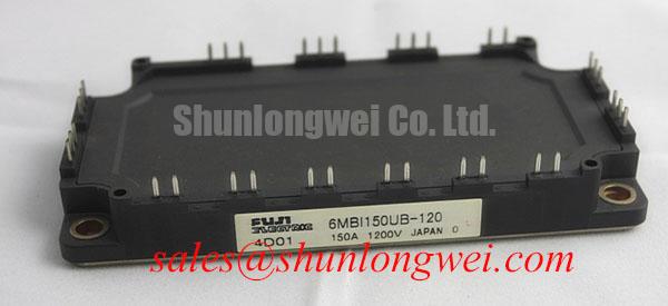
Fuji Electric 6MBI150UB-120-01: Initial Checks and Key Specifications
- Isolate the incoming supply, verify DC-link discharge with a suitable instrument, and disconnect external paths before comparing cold collector-emitter and gate-emitter readings.
- Check the module marking against 6MBI150UB-120-01, then compare the terminal arrangement and mounting interfaces with the equipment drawing.
- Inspect the heatsink contact surface, mounting hardware, and gate connections for contamination, looseness, or mechanical damage.
- Check the gate-driver supply and protection circuit before reconnecting the power stage; a damaged driver can compromise a replacement module.
The Fuji Electric 6MBI150UB-120-01 is a 1200 V, 150 A IGBT module. For a stopped power converter, the useful starting point is its electrical boundary and the condition of the surrounding circuit—not an assumption that matching current ratings establish interchangeability. The following specification card separates device ratings from the system-level checks discussed below.
| Technical parameter | Official Specification | Interpretation for integration |
|---|---|---|
| Collector-emitter voltage | 1200 V | Blocking-voltage rating; switching overshoot must be assessed separately. |
| Continuous collector current | 150 A at case temperature 80°C | A case-temperature-dependent rating, not an unrestricted equipment output current. |
| Collector-emitter saturation voltage | 2.10 V typical | Typical conduction characteristic, not a maximum loss guarantee. |
| Turn-off switching energy | 17.5 mJ typical | Operating-point-dependent turn-off energy, not total switching loss. |
| Short-circuit withstand time | 10 µs at 800 V | A conditional withstand characteristic, not a protection-delay setting. |
| IGBT junction-to-case thermal resistance | 0.13°C/W | Steady-state junction-to-case thermal resistance, not transient thermal impedance. |
Consult the model-specific datasheet for the remaining electrical test conditions, transient thermal curves, terminal drawing, mechanical dimensions, and mounting limits. Typical values should remain associated with their stated test conditions when comparing devices or estimating losses.
Benchtop Waveform Tuning: Mitigating Stress via Transient Thermal Impedance on 6MBI150UB-120-01
Capture the overload pulse duration and repetition pattern before estimating junction temperature. Design Consideration: the published 0.13°C/W junction-to-case value describes the steady-state thermal path; applying it directly to every brief pulse misses the time-dependent heating and cooling that determine peak junction temperature.
For an engineering calculation, build the loss waveform from conduction intervals and switching events at the actual operating point. Conduction loss follows instantaneous current and collector-emitter voltage, while switching loss depends on the measured event energies and their repetition. The 2.10 V typical saturation voltage and 17.5 mJ typical turn-off energy provide reference characteristics, but neither should be treated as constant throughout an overload cycle.
A manufacturer-supported multi-RC thermal model can translate that loss waveform into junction-temperature rise. Apply each change in dissipation to the model’s time response and superimpose the residual heating from preceding pulses. Add the measured case temperature at the specified reference location to obtain the estimated junction temperature. Preserve the model’s boundary conditions: a mathematical fit to junction-to-case impedance does not automatically describe the heatsink, interface material, or enclosure airflow.
On the bench, record case-temperature drift over repeated loading rather than judging the assembly from an isolated pulse. A cool starting case can conceal accumulated heat during a sustained duty cycle. If temperature continues rising between bursts, investigate the cooling path and duty pattern before changing gate resistance to improve a single waveform.
Keep voltage and current measurements time-aligned when examining switching energy. Probe delay, ringing, and measurement-loop pickup can distort the apparent overlap between voltage and current. Route gate-drive connections away from the high-current commutation path, and establish separation from switching conductors according to the equipment’s electrical and mechanical requirements.
Field Alert: Tighten mounting hardware to the applicable module and equipment specifications, and apply the thermal interface material uniformly rather than using extra torque to compensate for poor surface contact.
The Fuji Electric Power Semiconductor & IPM Modules resource provides manufacturer context for power-device documentation; use the exact module’s characteristics when correlating a thermal model with measured switching behavior.
Benchtop Waveform Tuning: Mitigating Stress via Sizing Braking Resistors and Chopper Transistors on 6MBI150UB-120-01
Trace the DC-link braking branch before attributing a deceleration overvoltage trip to the inverter module. Design Consideration: a braking chopper and resistor are system elements; their presence, connection, and control cannot be inferred from the 6MBI150UB-120-01 designation.
Where a motor drive returns mechanical energy to the DC link, resistor selection starts with the energy released during deceleration, the stopping interval, and the repetition of that event. The resistor must satisfy both pulse-energy and average-dissipation requirements. Its resistance also determines chopper current at the operating link voltage, so reducing resistance to accelerate discharge can increase semiconductor stress.
Evaluate the braking transistor against repetitive current, blocking voltage, switching energy, and its thermal operating envelope. Examine the resistor wiring and connection hardware as part of the current path: an intermittent connection can interrupt energy absorption without producing an obvious cold resistance fault. Record the DC-link rise, braking command, and branch current together to distinguish control timing from an open or overloaded dissipation path.
If the high-side driver uses bootstrap power, assess charge consumption over the longest interval without an effective recharge opportunity. The capacitor must support gate charge, driver quiescent consumption, and leakage while keeping the driver supply inside its operating limits. Include capacitor tolerance, temperature behavior, recharge-path impedance, and undervoltage-lockout behavior. The final capacitance and permissible duty pattern belong to the selected driver and switching sequence, not to the IGBT current rating.
Separate front-end topology from component naming when examining associated power stages. The 2MBI150U4H-170 is a separate power-module reference for evaluating another converter leg; it should not be treated as a passive rectifier or an automatic companion to this module. Any complementary stage needs its own circuit, drive, voltage, and thermal assessment.
A replacement comparison with 6MBI150U2B-060 likewise requires the exact voltage class, circuit configuration, terminal geometry, and switching characteristics to be checked. A similar model name or current designation does not establish a drop-in replacement. Industrial inverter welders and medium-frequency induction-heating supplies are potential compatibility-assessment examples, subject to their actual bridge arrangement, switching duty, cooling, and protection requirements.
Field Diagnostics & Commissioning: Common-Mode Transient Immunity in 6MBI150UB-120-01 Topologies
Measure gate-emitter voltage at the module connection during switching transitions, not only at the driver-board output. Design Consideration: common-mode displacement current and shared return-path inductance can disturb the voltage reaching the gate even when the controller command remains clean.
Use appropriately rated differential or isolated instrumentation and keep the measurement loop compact. Compare the commanded-off gate waveform with the switching-node transition and driver supply behavior. A brief disturbance may reflect coupling, return-path movement, supply collapse, or probe pickup; establish which signals move together before assigning the fault to the semiconductor.
Isolation withstand voltage, reinforced-insulation status, and common-mode transient immunity describe different properties. Assess them from the selected driver’s documentation and the complete insulation arrangement, including working voltage, transient exposure, creepage, clearance, and environmental conditions. A driver’s isolation-test rating does not establish reinforced insulation for the assembled converter, and a module blocking-voltage rating does not specify driver CMTI.
Where the original circuit uses negative gate turn-off bias, verify that the supply remains stable during commutation and that the gate-emitter excursions remain within device limits. Negative bias is not a substitute for a compact gate loop, controlled return routing, or a suitable driver. Preserve the intended gate-return reference and evaluate shielding arrangements against measured coupling rather than attaching shields indiscriminately to switching conductors.
Check protection timing across sensing, blanking, logic propagation, driver response, and controlled turn-off. The specified 10 µs short-circuit withstand time at 800 V is not an allowance to delay fault detection until that interval expires. Turn-off behavior also matters because rapid interruption of fault current can produce additional voltage stress.
For a broader diagnostic framework, the Power Electronics Masterclass connects device selection with gate-drive and protection checks. Keep the service measurements tied to this module’s circuit: thyristor trigger-current specifications and surge-current terminology are not substitutes for IGBT gate-drive and switching limits.
Assembly Integrity & Layout Architecture: Implementing Output Sinusoidal Filter vs dv/dt Reactor for 6MBI150UB-120-01
Compare the converter-output waveform with the waveform at the load terminals before selecting an output filter. Design Consideration: cable impedance discontinuities can produce reflected-wave overshoot, but its amplitude depends on edge speed, cable propagation, termination, and losses rather than a universal multiplication factor.
A dv/dt reactor or filter addresses transition steepness and associated cable stress; a sinusoidal filter aims to attenuate switching-frequency content more extensively. Selection therefore begins with the load’s insulation requirements, cable arrangement, fundamental frequency, carrier behavior, and allowable voltage drop. An output choke alone should not be assumed to produce the waveform of a complete sinusoidal filter.
Check filter current capability, magnetic heating, capacitor current, damping, and interaction with the drive’s control method. Added capacitance can change the current demanded from the inverter during switching. A quieter-looking load waveform is not sufficient evidence of reduced module stress if circulating current or filter resonance increases power-stage heating.
Inspect the physical current path after any filter or cable change. Keep outgoing and returning conductors arranged to limit unintended loop area, separate sensitive gate connections from output wiring, and maintain the equipment’s required insulation distances. Confirm mechanical support so cable forces do not load the module terminals or disturb the heatsink interface.
Commission with the intended cable and load configuration, observing output overshoot, gate behavior, current, and temperature as loading increases. If an oscillation appears after a filter change, compare its timing with switching events and control activity before altering damping or carrier settings. Release the equipment only after the modified output network remains compatible with the drive’s protection, thermal behavior, and operating range.