

Content last revised on September 10, 2026
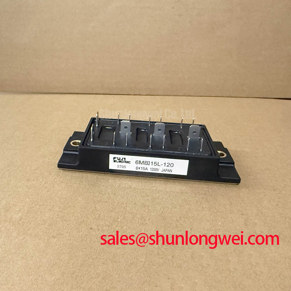
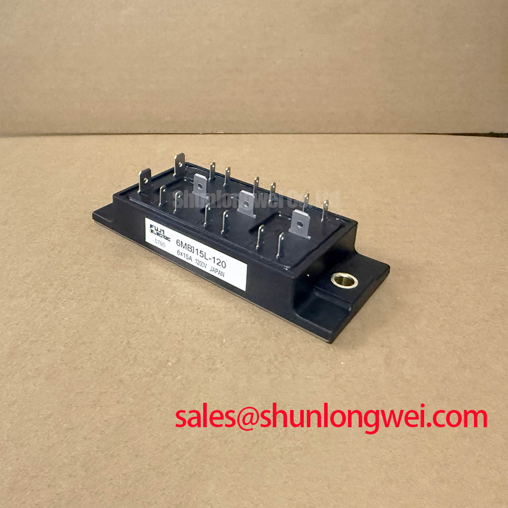
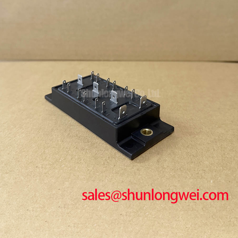
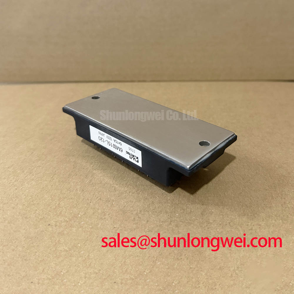
Before installation, verify the equipment nameplate and the removed module’s terminal arrangement against the original drive documentation, then confirm that the replacement device ratings are 1200 V and 15.0 A. The 6MBI15L-120 is a Fuji Electric power semiconductor Module with these stated ratings. The system integrator should verify the original inverter topology, gate driver interface, mounting pattern, insulation arrangement, and control protection settings before energizing the DC bus.
| Parameter | Declared Value | Classification |
|---|---|---|
| Product model | 6MBI15L-120 | Official product identification |
| Manufacturer | Fuji Electric | Official manufacturer identification |
| Rated voltage | 1200 V | Official Specification |
| Rated current | 15.0 A | Official Specification |
| Package category | Module | Official Specification |
Assembly Integrity and Layout Architecture: DC Bus Headroom Derating for 6MBI15L-120
The voltage boundary is the first non negotiable review point for a 6MBI15L-120 replacement. Its declared rating is 1200 V, and this value must be evaluated against the complete operating DC bus rather than only the nominal supply label. Bus voltage can rise during regeneration, deceleration, supply variation, and switching events. The device rating does not by itself establish an allowable system bus voltage, expected switching overshoot, or a required derating percentage. Those values are determined by the original circuit, measured waveforms, and the equipment designer’s protection strategy.
Design Consideration: keep the high current commutation path physically compact so that the DC link capacitor, module power terminals, and return conductors form the smallest practical loop. A laminated or closely coupled bus arrangement can reduce parasitic inductance, helping suppress turn off voltage overshoot. Confirmation requires measurement at the relevant power terminals with suitable high bandwidth probing while the actual load and switching conditions are present. A controller that appears stable at light load can show materially different transient behavior during acceleration, rapid torque reversal, or regenerative braking.
For compact industrial inverter repair, inspect the bus capacitor condition, terminal hardware, copper discoloration, and signs of localized heating before fitting the module. Mechanical damage, loose terminals, contaminated contact surfaces, or a distorted heat spreader interface can alter both electrical and thermal behavior. A resistance check between external power connections with the unit isolated may help identify an obvious bus short, but it cannot establish semiconductor switching integrity or protection performance. Gate drive signals and power stage waveforms should be compared with a known good channel where that comparison is available.
Altitude introduces another system level consideration. Terrestrial neutron exposure and single event burnout discussions are sometimes associated with high voltage semiconductor operation at elevated locations. No FIT value, altitude threshold, or single event burnout rate is established here for the 6MBI15L-120. Engineers assessing equipment above 2000 m should treat this as a Design Consideration and consult the original equipment environmental requirements, insulation coordination documentation, and manufacturer approved qualification data. The practical task is to preserve measured DC bus voltage headroom under the actual site conditions rather than infer a reliability number from nominal altitude alone.
💡 Pro Tip: Tighten all power and mounting hardware using the original equipment torque specification, because uneven contact pressure or a loose bus connection can distort thermal transfer and create switching overshoot that is not visible during a basic continuity test.
Where braking energy is handled through a chopper and resistor assembly, the service check should include the braking resistor, chopper control signal, DC bus sensing path, and capacitor bank. A malfunction in any of these connected circuits can permit bus voltage escalation even when the power module itself is functional. Fuji Electric publishes related background on brake chopper IGBT modules, which can help engineers distinguish the role of a power switch from the wider regeneration control arrangement.
6MBI15L-120 Operational Boundaries: Evaluating SCSOA Overcurrent Protection Limits
Short circuit protection must be treated as a property of the complete power stage, gate driver, sensing circuit, controller response, and bus layout. The stated 1200 V and 15.0 A ratings do not provide a verified short circuit withstand interval, short circuit safe operating area curve, gate charge value, or desaturation threshold for this specific module. For that reason, a stated sub 10 microsecond detection target cannot be presented as an official 6MBI15L-120 specification without the corresponding manufacturer documentation.
Engineering Recommendation: evaluate the protection chain from fault detection through gate discharge and final current interruption. Type I and Type II fault terminology can describe different short circuit conditions in power electronics, but the applicable event classification must match the original drive architecture. Engineers should capture the collector current, DC bus voltage, gate voltage, and fault timing during controlled validation. This verifies whether protection reacts before electrical and thermal stress exceeds the boundaries demonstrated by the original system design.
Two stage soft turn off is often considered where an abrupt gate discharge could produce a damaging inductive voltage transient. It is a Design Consideration rather than a universal repair instruction. The suitable gate discharge profile depends on the driver capability, bus inductance, load current, control timing, and measured voltage margin. If a replacement board or revised driver is used, validate the behavior with the actual module and load rather than assuming that a slower or faster turn off is inherently safer.
High side driver supply integrity also deserves direct inspection. Bootstrap capacitor sizing depends on the installed driver’s gate charge demand, quiescent current, allowed supply variation, PWM timing, and recharge interval. No gate charge or driver supply requirement is declared for this module in the available official parameter set. The system integrator should therefore use the original gate driver documentation and verify supply voltage at the driver during operating duty cycles. A supply that collapses during a long high side command can create incomplete gate drive, while an unstable reference path may produce misleading oscilloscope results.
During equipment repair, verify current sensor polarity, fault comparator routing, isolation barrier condition, and controller interlock behavior before applying full bus power. If the drive has a precharge circuit, confirm that it establishes the intended capacitor charging sequence and that the main contactor or switching path closes correctly. These checks are relevant to compact inverters and high speed CNC spindle drives, but they do not establish that this module is approved for every implementation of those equipment categories.
For context on related integrated power semiconductor arrangements, the Fuji Electric RC IGBT module information is useful when reviewing how device functions can vary across module families. It should not be used to infer undocumented characteristics of the 6MBI15L-120.
6MBI15L-120 Operational Boundaries: Optimizing Gate Drive Loop Geometry to Prevent Limits
Gate loop geometry has a direct influence on switching repeatability. The gate drive circuit should return through the intended low current reference path rather than sharing a long section of the main power current return. Shared inductance can create a voltage disturbance during changing load current, and that disturbance can alter the effective gate to emitter voltage seen by the switching device. The result may be ringing, delayed switching, unexpected turn on, or unequal stress between channels, depending on the original circuit topology.
Design Consideration: separate sensitive gate drive conductors from high current bus conductors wherever the original layout permits, minimize loop area, and retain the driver reference architecture specified by the equipment design. Do not infer the existence of a dedicated auxiliary emitter connection, Kelvin connection, internal clamp, or a particular terminal arrangement from the product name alone. The original terminal drawing and equipment schematic remain the controlling references for connection identification.
When diagnosing oscillation, inspect the gate resistor network, driver output stage, isolation supply return, connector seating, and nearby control grounding. A repetitive gate waveform anomaly may indicate excessive parasitic coupling, an unsuitable replacement component value, degraded driver circuitry, or probe grounding error. Verify with a properly referenced measurement method and compare the suspect phase with an unaffected phase if the equipment arrangement allows it. Avoid interpreting a single waveform feature as proof of one specific failure cause.
A repair engineer considering a lower voltage member of the same naming family can review 6MBI15L-060 as a separate product reference. This is not a direct substitute recommendation. Its electrical rating, terminal pattern, internal configuration, control compatibility, and application suitability must be checked independently against the removed unit and the original equipment documentation.
The associated power stage should also be reviewed as a whole. For example, 6MBI300U-120 is a separate module reference that may appear in related power conversion sourcing searches, but its stated product identity does not establish electrical interchangeability with the 6MBI15L-120. Current class, voltage class, topology, driver requirements, mechanical interface, and thermal arrangement require independent verification.
Thermal installation should be handled with the same discipline as electrical layout. Inspect the heatsink flatness, remove hardened interface residue without damaging surfaces, and apply the thermal interface material according to the original assembly process. The supplied information does not state a module thermal resistance, junction temperature limit, baseplate construction, interface material thickness, or mounting torque. Pulse temperature margin and transient thermal impedance must therefore be evaluated from the original manufacturer documentation and measured system duty, not estimated from the 15.0 A current rating alone.
6MBI15L-120 Circuit Protection and Reliability: Calibrating Suppression of Miller-Induced Gate Voltage Spikes
Fast voltage transitions across a power switch can couple energy into an off state gate path through capacitance within the circuit. This can raise gate voltage and create a risk of unintended turn on in a bridge leg. The exact capacitance values, Miller plateau charge, internal gate resistance, and switching speed data for the 6MBI15L-120 are not included in the declared official parameter set. They should not be assumed from another Fuji Electric module family or from general IGBT behavior.
Engineering Recommendation: inspect whether the original driver uses an active Miller clamp, a defined off state gate path, split turn on and turn off impedance, or another anti cross conduction method. Any negative gate bias level must come from the original driver and module documentation. A negative bias range should not be selected from generic practice alone because the allowed gate voltage boundaries and driver isolation requirements are system determined. Validate gate voltage at the module connection during high dv over dt switching and confirm that commanded off devices remain off under the most demanding practical operating condition.
Protection verification should include dead time control, driver undervoltage lockout behavior, fault reset sequence, and logic interlocking between complementary commands. These functions work together. An active clamp cannot compensate for a controller timing fault, and a suitable dead time strategy cannot correct a poorly referenced gate return. Where waveforms show repeated ringing or apparent cross conduction, isolate the investigation into power loop, driver supply, control command, and measurement setup rather than replacing parts without evidence.
For long term service planning, focus on objective observations: recurring alarm codes, bus voltage records, heatsink condition, fan operation, terminal retention, and captured switching waveforms. No service life hours, failure rates, insulation reliability figures, EMC approval, or field failure statistics are claimed for this module. Engineers who need a structured troubleshooting framework can consult the Field Engineer’s Handbook for measurement led fault analysis practices. Final acceptance should remain based on the original equipment requirements and controlled functional testing.