Content last revised on September 10, 2026
Assembly Integrity & Layout Architecture: Implementing DC Bus Operating Voltage Headroom Derating for 7MBP100TEA060
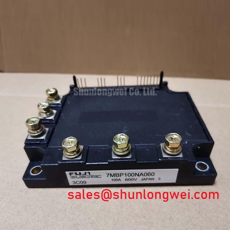
Check the module marking against the equipment documentation, inspect the power terminals and housing for mechanical damage, then verify the cold electrical condition before connecting the drive. The 7MBP100TEA060 is a Fuji Electric PIM power module specified for inverter and brake integration in industrial power conversion equipment.
| Parameter | Official Specification | Engineering Relevance |
|---|---|---|
| Collector emitter voltage | 600 V VCES | Defines the rated blocking voltage boundary for the IGBT power stage |
| Rated collector current | 100 A IC | Supports evaluation in medium duty and heavy duty motor drive applications, subject to thermal conditions |
| Typical saturation voltage | 2.10 V VCE(sat) | Used when estimating conduction loss under the manufacturer’s specified test conditions |
| Temperature monitoring | Integrated RTC thermistor included | Provides a resistance based temperature feedback path for system monitoring |
| Package style | PIM, 7 pack | Combines inverter and brake functions in a compact module arrangement |
The listed electrical values are official product specifications supplied for this model. Actual allowable current depends on switching frequency, case temperature, thermal interface quality, cooling hardware, modulation conditions and the complete drive operating profile. The system designer should confirm the applicable Fuji Electric thermal and safe operating area data before approving the module for continuous service.
Begin assembly verification with the DC bus voltage, braking circuit configuration and switching waveform rather than relying only on the nominal AC input. The 600 V VCES rating is an official device boundary, not a target operating voltage. Bus ripple, regenerative energy, commutation overshoot and control faults can all raise the instantaneous collector emitter stress above the measured steady state bus value.
Altitude related reliability requires documented evidence from the complete equipment design. Reduced air density can affect external insulation coordination and cooling performance, while terrestrial neutron exposure may be relevant to high voltage semiconductor reliability at elevated installation sites. No product specific SEB FIT rate or altitude derating curve should be inferred without an authoritative Fuji Electric reliability document or an applicable system qualification report. A suitable Design Consideration is to evaluate the installed DC bus, transient peak voltage, creepage, clearance, cooling capacity and protection response together, then validate the result in environmental and switching tests.
Keep the high current commutation path compact and physically controlled. The positive bus, module terminals and DC link return should follow a low-loop-area geometry that limits stray inductance. Separate control wiring from power switching conductors, and avoid routing thermistor wiring through areas with strong switching field coupling. Inspect terminal flatness, fastener seating and thermal interface contact during assembly. If a replacement is being assessed, compare the complete pinout, brake topology, electrical ratings, mounting arrangement and drive firmware assumptions with the original documentation. The related 6MBI100L-060 can be reviewed as a separate, objectively specified module option, not as an automatic substitute.
For field commissioning, record the DC bus waveform during acceleration, deceleration and fault recovery. A waveform that approaches the device voltage boundary may indicate insufficient clamping, excessive loop inductance or an incorrectly timed brake circuit. Confirm the measurement bandwidth, probe connection and reference point before making a repair decision. Fuji Electric’s technical resources at Fuji Electric Global Power Semiconductor Technologies provide useful manufacturer context for power semiconductor evaluation.
Field Diagnostics & Commissioning: Active Miller Clamp Implementation in 7MBP100TEA060 Topologies
During gate drive commissioning, check the gate emitter waveform directly at the module terminals. A control signal that appears correct at the driver board may show ringing or unwanted gate elevation at the power module because of common emitter inductance and the physical separation between driver and module. The 7MBP100TEA060 specification confirms the power device ratings, but the exact gate voltage limits, gate resistance values, switching conditions and protection timing must be taken from the applicable manufacturer documentation.
An active Miller clamp is a Design Consideration when high collector voltage slew during turn off creates a risk of unintended gate charging. Its effectiveness depends on the driver topology, sensing reference, propagation delay, gate loop impedance and the module’s actual switching behavior. Do not assume that a negative gate bias is required or suitable for this specific installation without confirming the driver and Fuji Electric application data. If the system uses a negative gate supply, the integrator should verify the permitted gate emitter range, startup sequence and fault state under all operating conditions.
Cross conduction troubleshooting should include simultaneous observation of the upper and lower switch gate emitter signals, the phase node and the driver fault output. Unexpected overlap may involve timing, isolation behavior, gate loop coupling, auxiliary supply disturbance or measurement error. Replace speculative diagnosis with a known good waveform comparison and controlled low energy testing before returning the drive to full power.
When modules are paralleled, static current sharing should be assessed from the actual VCE(sat) distribution, thermal coupling and busbar resistance. A positive temperature coefficient can support balancing behavior in some operating regions, but it does not remove the need for symmetrical electrical paths and matched gate drive timing. The 7MBP100TEA060 has a typical saturation voltage of 2.10 V; engineers should use the manufacturer’s test conditions when comparing this value with measured production results.
Field Alert: Disconnect the DC link and verify the discharge state before inserting or removing gate driver and thermistor connectors.
7MBP100TEA060 Circuit Protection & Reliability: Calibrating Auxiliary Emitter Return Trace Separation
The auxiliary emitter return should be treated as a measurement and gate drive reference, not as an extension of the high current power return. Sharing a narrow control reference path with a rapidly changing emitter current can introduce voltage error at the driver, causing gate waveform distortion or apparent switching instability. The required separation is system dependent and should be confirmed from the module terminal arrangement and the drive schematic.
Review the copper geometry from the module terminals to the driver, paying attention to parallel runs, return path area and connection points around current sensors. The thermistor circuit should be routed as a low noise measurement path and checked for continuity, connector contact quality and plausible resistance change during controlled thermal testing. An open or unstable RTC signal may cause a protective shutdown, but the diagnostic conclusion should be based on measured resistance and the controller’s documented threshold behavior.
Protection coordination should cover overcurrent detection, short circuit response, gate supply supervision, undervoltage behavior and thermal feedback. The module’s 100 A IC value is an official rated collector current specification, not a short circuit withstand guarantee. Peak fault current, interruption time and repetitive fault capability require the relevant device curves and system test evidence.
For a failed drive, compare all phase legs rather than testing only the suspected module. Inspect the gate emitter voltage, collector emitter leakage behavior under an appropriately controlled test method, thermistor continuity and the condition of adjacent driver components. A damaged module can be a consequence of a driver fault, bus transient or cooling problem, so replacing the power module without checking those surrounding conditions may lead to another failure.
Preventing Spurious Faults: DC Link Capacitance Bank Layout and Low ESR Guidelines for 7MBP100TEA060
Place the high frequency portion of the DC link close to the switching bridge and keep the positive and negative paths broad, short and geometrically balanced. The switching transient can be understood through the relationship between DC bus voltage, stray inductance and current slew: additional inductive voltage appears whenever the current changes rapidly. The peak must be measured at the module terminals and evaluated against the rated 600 V VCES boundary, including regenerative and fault conditions.
Capacitor selection is a Design Consideration governed by ripple current, frequency spectrum, thermal rise, impedance across the relevant frequency range and the physical connection to the commutation loop. A low ESR label alone does not confirm effective transient control if the mounting path adds substantial inductance. Snubber selection should be based on double pulse testing or an equivalent validated switching test, with voltage, pulse energy and thermal stress checked for the actual operating duty.
Use a planar or otherwise symmetrical busbar arrangement where practical, and avoid placing the brake path so that its current shares an uncontrolled loop with the inverter phase legs. Check the DC link with a properly connected differential probe during motor acceleration, regenerative braking and abrupt load changes. If the measured peak changes significantly when probe placement changes, the measurement setup may be contributing an artifact.
Preventive verification can include torque and flatness checks at power terminals, inspection of capacitor connections, thermal interface review and a comparison of all phase switching waveforms. Engineers evaluating the module in broader industrial systems can consult the Industrial Applications reference for application context. Additional power semiconductor background is available from SanRex Sansha Electric Power Semiconductor Modules. These references do not replace the Fuji Electric documentation or the system designer’s measured voltage, thermal and protection validation.