
Content last revised on October 11, 2026
PM100CSA060 Thermal Electrical Optimization with Low Inductance DC Busbar Layout
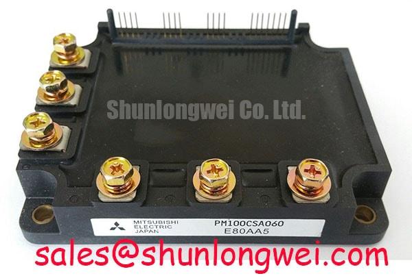
When a commercial string inverter or microgrid energy storage converter shows excessive turn off overshoot, start at the commutation path rather than changing the power module immediately. The PM100CSA060 is identified as a Mitsubishi Electric IPM Module with a 600.0 V rated voltage and 100.0 A rated current. These are official product specifications and define the component rating reference, while the usable switching margin remains dependent on the complete power stage, cooling arrangement, switching conditions, and protection design.
The switching transient is governed by the stray inductance in the DC link and power commutation loop. In practical terms, the peak collector emitter voltage rises as the DC bus voltage combines with the inductive voltage generated by current change. The relationship can be described naturally as Vpeak = VDC + Lσ multiplied by di/dt. This is an engineering calculation model, not an additional factory rating for the PM100CSA060. The measured peak must remain within the system’s validated electrical boundary after temperature, load current, gate timing, and wiring variation have been considered.
A laminated busbar or closely coupled planar conductor arrangement can reduce the commutation loop area. Place the high frequency DC link capacitor close to the module power terminals, keep the positive and negative current paths adjacent, and avoid routing the return conductor around control boards or mounting openings. Clearance must still satisfy the insulation, contamination, creepage, and service requirements of the complete inverter enclosure. A low inductance target such as less than 25 nH may be used only as a project specific engineering objective when supported by measured impedance and switching results; it is not an official PM100CSA060 parameter.
During commissioning, use a properly rated differential voltage probe and a current probe with bandwidth suitable for the switching edge. Compare turn off voltage, current decay, ringing frequency, and temperature at several operating points. If the overshoot changes sharply when the probe ground arrangement changes, the measurement loop may be influencing the result. A snubber can be assessed after the physical commutation path has been optimized. Its capacitance, resistance, pulse energy, and thermal dissipation should be selected from measured waveforms and switching loss calculations rather than copied from another module.
The Mitsubishi Electric power semiconductor resource provides manufacturer level context for power devices and module technologies. For a related system topology, engineers may also review the CM200DXDX1 24A as a neutral reference for the front end or complementary power stage. Compatibility must be evaluated from voltage, current, switching, thermal, terminal, and control requirements rather than physical appearance alone.
Transient Dynamics and Electrical Design for PM100CSA060 Gate Loop Symmetry
The gate drive loop should be treated as a high speed power circuit. Separate the control return path from the main high current emitter return wherever the device interface provides a distinct auxiliary or Kelvin reference. Shared copper can introduce emitter mutual coupling, causing the gate driver to respond to voltage developed by load current instead of the intended gate signal. The result may appear as ringing, uneven switching between positions, or sensitivity to cable placement.
Keep the outgoing gate path and its return path close together, with a compact loop and controlled connection to the driver output stage. Avoid routing the gate trace beside high dv/dt collector or switching node copper for long distances. The driver supply bypass network should be placed according to the driver manufacturer’s layout requirements. Any isolation barrier, gate transformer, or isolated driver must be checked for common mode transient performance at the actual switching edge.
Desaturation protection can provide a fast response to abnormal conduction conditions, but its sensing path must be coordinated with blanking, filtering, and the module’s switching behavior. A short circuit detection interval such as less than 3 microseconds is a design objective sometimes specified for a particular protection architecture; it is not confirmed here as a PM100CSA060 factory specification. Designers should select the protection timing from the gate driver data, measured short circuit response, device short circuit withstand information, and the required system shutdown sequence.
A two stage soft turn off strategy can reduce the voltage step during a protection event. The first stage removes the normal gate drive promptly, while the second stage controls the remaining current transition to limit inductive overshoot. The actual gate resistance, clamp voltage, negative bias, and timing belong to the driver and system design. They should be tuned with a current probe and differential voltage probe while checking the gate emitter waveform directly at the module terminals.
Common mode ground bounce should be evaluated at the driver isolation boundary and at the auxiliary emitter reference. A control waveform that appears clean at the driver board may be distorted at the module because of connector inductance or separate chassis return paths. The Mitsubishi Electric high voltage module information offers useful manufacturer context, but the exact gate drive and protection interface must follow the documentation applicable to the purchased device and driver combination.
🔧 Bench Diagnostic: Remove DC bus power and verify the discharge state before disconnecting any gate drive or control connector.
Field Diagnostics and Commissioning for Damping Tail Current Oscillations
Turn-off tail current oscillation should be examined together with the antiparallel freewheeling path, commutation inductance, gate resistance, and reverse recovery behavior. A high reverse recovery current or abrupt di/dt can couple into the DC link and gate loop, producing ringing that may be mistaken for a defective IPM. The waveform should be captured at the module power terminals with a short measurement path and then compared against the same circuit at reduced current.
Reverse recovery is affected by junction temperature, forward current, commutation voltage, gate timing, and the characteristics of the paired switching path. If the current probe shows a sharp recovery peak, inspect the physical loop before changing gate resistance. Long leads between the module and DC link capacitor can store additional magnetic energy, while asymmetric phase layout can cause different overshoot on otherwise identical legs.
An RC snubber may reduce high frequency ringing when it is placed across the correct switching nodes and selected for the actual pulse energy. The resistor must tolerate repetitive pulse power, and the capacitor must maintain suitable electrical behavior at the operating frequency and voltage. Snubber losses should be included in the thermal assessment. A snubber fitted without observing the voltage and current phase relationship can increase loss without resolving the original resonance.
Turn on gate resistance is another possible tuning variable. A higher resistance can slow the current transition and reduce some ringing, but it may increase switching loss and affect thermal balance. A lower resistance can shorten the transition while increasing di/dt and voltage stress. The appropriate value is therefore a typical starting point for bench tuning, not a universal prescription for this model. Use double pulse or controlled switching tests to compare turn on loss, reverse recovery current, gate waveform, and peak voltage under the intended operating conditions.
Electromagnetic emissions should be assessed after the power loop and gate loop have been stabilized. A component by itself does not possess independent system level CISPR or EN 55011 compliance. Cable routing, enclosure bonding, filter topology, chassis construction, and the complete converter assembly determine the final result. For broader service methods covering waveform capture, failure analysis, and reliability checks, engineers can consult the Field Engineer’s Handbook.
For urgent service evaluation, the PM50RL1B120 may be reviewed as a separate Mitsubishi Electric module reference. It should not be treated as a direct replacement unless the equipment engineer confirms voltage class, current capability, mechanical mounting, terminal arrangement, gate drive behavior, protection interface, thermal path, and control compatibility.
Field Diagnostics and Commissioning for Mechanical Stress Control
Mechanical installation can alter electrical reliability when terminal hardware transfers leverage into the module body or busbar assembly. Before tightening the main power connections, align the busbar naturally with the terminal faces and confirm that no external conductor is forcing the terminal sideways. Thread engagement, washer selection, conductor flatness, and support spacing should be checked as an assembly rather than corrected by pulling the busbar into position with the screw.
Thermal cycling can expose installation stress that is not visible during a cold inspection. Copper conductors expand differently from the module housing, heatsink, and enclosure support. A rigid busbar with no controlled mechanical accommodation can load the terminal joint during temperature changes or vibration. The design team should provide mechanical support close to heavy conductors while preserving the electrical loop geometry established during switching validation.
When the module is mounted to a heatsink, inspect the contact surface for contamination, burrs, warping, or trapped debris. The thermal interface method must follow the applicable mechanical documentation and the material supplier’s process requirements. Apply clamping force evenly across the mounting points and use the specified hardware sequence. If a mounting torque is not confirmed in the relevant Mitsubishi Electric documentation, it should not be invented from a visually similar module.
During service inspection, look for displaced washers, thread damage, loosened terminal hardware, cracked soldered joints on attached busbars, and marks showing that the conductor has moved relative to the housing. These observations do not prove a single failure cause, so correlate them with phase resistance, insulation checks, gate waveform behavior, and thermal history. Any electrical test must be carried out with the DC link safely discharged and with the module isolated from sensitive control circuitry.
For commercial string inverter and microgrid energy storage integration, the PM100CSA060 should be evaluated as part of the complete switching leg, not as an isolated current rating. Confirm the required DC bus range, transient voltage margin, switching frequency, cooling capacity, protection sequence, and enclosure environment. Mechanical alignment, low inductance layout, gate loop symmetry, and controlled commissioning should be verified together before applying full operating power.