Content last revised on September 10, 2026
Symmetrical Busbar Geometry for High-Current Parallel Module Arrays
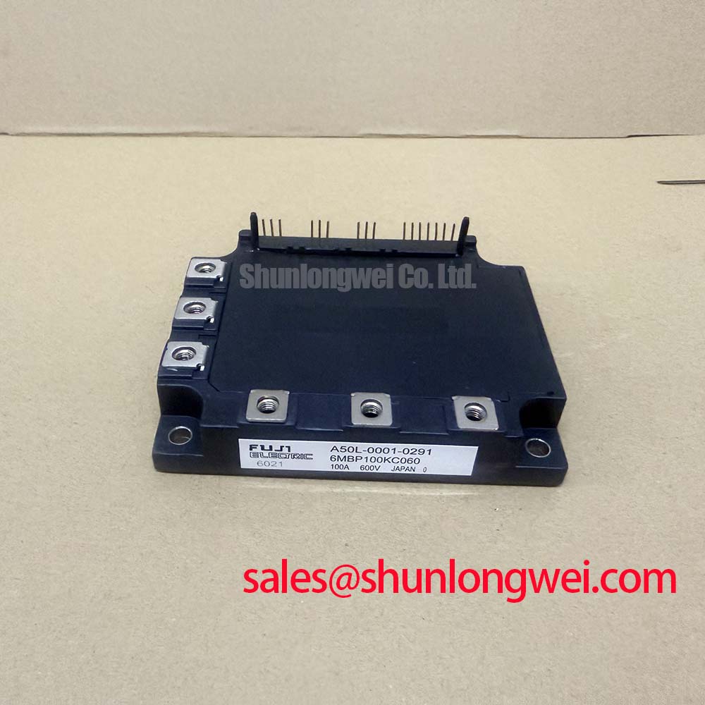
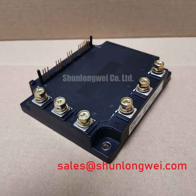
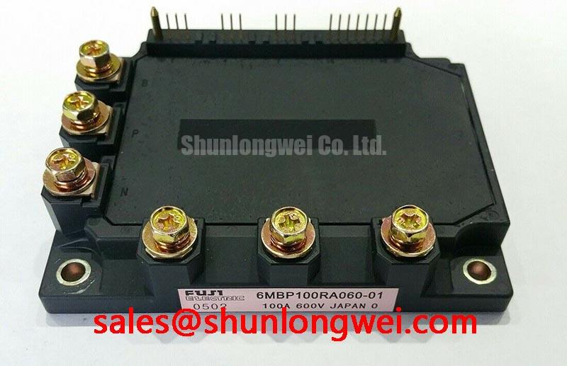
When conducting incoming QA and static bench verification on the 6MBP100RA060-01 Intelligent Power Module (IPM) from Fuji Electric, verifying mechanical planar alignment and terminal coplanarity across the molded baseplate forms the baseline of our physical inspection. Rated at a collector-emitter voltage of VCES = 600.0V (Official Datasheet Specification) and a nominal continuous collector current of IC = 100.0A at 25°C (Official Datasheet Specification), this 6-pack inverter topology module features integrated gate drive logic and built-in protection. In high-power variable frequency AC motor drives requiring scaling beyond 100A, systems occasionally parallel module phases or split power runs across symmetrical bus structures. Achieving static current balance between parallel channels relies fundamentally on the positive temperature coefficient of the collector-emitter saturation voltage VCE(sat) at high current densities.
During cold-state bench testing with a curve tracer or high-current pulsed source, a typical unmounted 6MBP100RA060-01 demonstrates a nominal VCE(sat) of 1.70V to 2.10V at 100A at an ambient junction temperature of 25°C. When junction temperatures rise under heavy duty drive cycles toward 125°C, VCE(sat) shifts upward, forcing current to redistribute naturally into cooler parallel paths. However, static saturation matching is ineffective if the dynamic layout introduces path impedance disparities. Symmetrical busbar geometry must enforce identical branch resistance and loop inductance down to sub-milliohm and nanohenry tolerances. Busbar runs must maintain strictly balanced track lengths, matching copper cross-sections, and equidistant connection points to ensure that neither parallel leg absorbs a disproportionate surge during hard switching commutations.
💡 Bench Tip: Before mounting, perform incoming cold-state checks with a digital multimeter in diode-check mode across the output terminals (U, V, W) to DC negative (N) and DC positive (P). Measure the anti-parallel free-wheeling diode (FWD) forward voltage drop VF across all six internal switches. At 25°C bench temperature, VF should measure between 0.42V and 0.58V under low meter test current (approx. 1mA). An internal branch divergence exceeding 50mV across arms often indicates thermal stress or silicon degradation from prior handling.
For systems undergoing retrofits or architectural re-evaluations where dual-pack configurations are preferred over integrated 6-pack modules, engineers frequently review the 2MBI150-060 half-bridge module, which provides dual 150A/600V switches in an isolated industrial housing. To inspect official packaging standards and internal drive protection mechanics across Fuji architectures, reference the Fuji Electric Power Semiconductor & IPM Modules technical documentation.
| Parameter | Symbol | Specification / Condition | Engineering Status |
|---|---|---|---|
| Collector-Emitter Breakdown Voltage | VCES | 600.0V (Tj = 25°C) | Official Datasheet Specification |
| Continuous Collector Current | IC | 100.0A (Tc = 25°C, Continuous) | Official Datasheet Specification |
| Pulsed Collector Current | ICP | 200.0A (1ms pulse width) | Official Datasheet Specification |
| Isolation Voltage (Terminal to Base) | Viso | 2500V AC (1 Minute, 50/60Hz) | Official Datasheet Specification |
| Module Mounting Screw Torque | M5 | 2.5 to 3.5 N·m | Design Consideration |
DC-Link Capacitance Bank Layout and Low-ESL Busbar Interconnection Techniques
In heavy-duty variable frequency AC motor drive applications, fast IGBT turn-off under full load induces steep di/dt transitions exceeding 1500 A/µs. When high-current transitions interact with DC-link parasitic loop inductance Lσ, severe overvoltage spikes are generated across the power terminals P and N. The transient collector-emitter voltage equals the instantaneous DC-link voltage plus the inductive kick derived from parasitic inductance multiplied by the rate of current decay. For a standard 400V DC operating rail, keeping peak voltage overshoot safely below the 600V VCES threshold mandates an aggregate parasitic loop inductance Lσ of less than 25nH across the high-frequency commutation path.
Minimizing this loop inductance requires laminated planar busbars where positive and negative copper plates are separated by an ultra-thin insulating dielectric such as polyimide or high-temperature Nomex. Running forward and return DC currents in tight parallel sheets forces magnetic flux cancellation, minimizing loop area. High-frequency polypropylene snubber film capacitors (typically 0.47µF to 2.2µF, 630V DC ratings) must be installed directly across the physical module terminals P and N with ultra-short leads. Avoid lengthy interconnects between the primary electrolytic bulk capacitance bank and the module terminals, as excessive trace length isolates the snubber during microsecond commutation events.
For higher voltage or dual-stage conversion platforms featuring separate brake and 3-phase rectifier stages, engineers can examine complementary assemblies like the 7MBI100U4E-120-50, which incorporates input rectification, chopper, and inverter stages in a single unified footprint. For further details on monolithic compact power integrations, review the Fuji Electric PIM (Power Integrated Module) 7-Pack platform specifications.
⚠️ Field Alert: Dead-time shoot-through prevention must be maintained within the host DSP/microcontroller firmware. While the 6MBP100RA060-01 incorporates built-in short-circuit (SC) and over-current (OC) shutoff circuitry, relying on internal fault suppression for repetitive bridge shoot-through conditions accelerates dielectric aging. Enforce an external hardware/firmware dead-time buffer of at least tdead = 2.0µs to 2.5µs (Design Consideration) between high-side and low-side switching signals to prevent cross-conduction during thermal extremes.
Thermal Time Constants (tau_i) and Peak Junction Temperature Margin Calculation
Heavy-duty AC drive profiles subject the power silicon to cyclical pulsed overloads during direct motor starting, dynamic braking, and mechanical stall events. Accurately determining whether the module operates within safe thermal margins requires evaluating the transient junction-to-case thermal impedance Zth(j-c) rather than relying solely on steady-state thermal resistance Rth(j-c). The thermal path across the IGBT silicon die, solder layer, Direct Copper Bonded (DCB) ceramic substrate, and copper baseplate is modeled using a multi-order Foster or Cauer RC network characterized by discrete thermal time constants τi ranging from 1ms up to 100ms.
During short locked-rotor current pulses (e.g., 150% to 200% load lasting 1 to 3 seconds), transient heat remains primarily trapped in the immediate silicon and DCB thermal mass before conducting out to the external heatsink. The junction temperature calculation must account for the accumulation of steady-state heat sink temperature, temperature rise across the thermal interface material (TIM), and the dynamic peak power pulse: Tj(peak) = Tsink + Ploss(avg) × Rth(c-s) + Ploss(pulse) × Zth(j-c)(tpulse). To ensure long-term industrial reliability, the calculated Tj(peak) should maintain at least a 25°C engineering safety margin below the absolute maximum continuous junction rating of 150°C (Official Datasheet Specification).
Comprehensive failure analysis methodologies, thermal resistance measurement protocols, and bond-wire lift validation tests are detailed in the Field Engineer’s Handbook, which serves as a technical benchmark for field reliability assessments.
| Thermal Characteristic | Symbol | Value / Condition | Identity Status |
|---|---|---|---|
| IGBT Thermal Resistance (Junction to Case) | Rth(j-c)_IGBT | 0.40 °C/W max per element | Official Datasheet Specification |
| FWD Thermal Resistance (Junction to Case) | Rth(j-c)_FWD | 0.90 °C/W max per element | Official Datasheet Specification |
| Contact Thermal Resistance (Case to Fin) | Rth(c-f) | 0.05 °C/W (with 1.0 W/m·K grease) | Design Consideration |
| Maximum Operating Junction Temperature | Tj(max) | 150°C | Official Datasheet Specification |
| Recommended Operating Case Temperature | Tc(rec) | -20°C to +100°C | Typical Starting Point |
PCB Symmetry Considerations for Dual IGBT Half-Bridge Switching Paths
The internal control interface of the 6MBP100RA060-01 integrates high-speed level shifting, under-voltage lockout (UVLO), and localized gate drive stages. However, external PCB layout across the input control connector pins (VLA, VHA, INU, INV, INW, etc.) dictates switching noise immunity. A common error in industrial drive layout is routing control signal grounds together with high-current power return lines. High emitter di/dt across shared trace inductance induces spurious voltage spikes that can corrupt logic levels, trigger false UVLO fault sequences, or cause gate oscillation.
To preserve signal integrity, the auxiliary Kelvin emitter and power ground return paths must remain strictly segregated on the PCB. The logic power supplies (typically 15V DC nominal for VCC) driving high-side optocouplers or isolated gate buffers must have dedicated decoupling capacitors located within 5mm of the IPM control pins. Use low-ESR ceramic capacitors (0.1µF to 1.0µF) in parallel with low-impedance electrolytic capacitors (10µF) across each isolated control rail. Shield control traces with solid ground planes beneath the routing layer, avoiding any parallel routing of signal traces alongside the high-voltage inverter output lines (U, V, W) to eliminate capacitive dV/dt cross-coupling.
Bench validation of replacement modules before field integration requires complete static pin isolation verification. Using a calibrated high-voltage insulation tester, apply 500V DC between the interconnected signal pins and the isolated metal baseplate. A healthy 6MBP100RA060-01 module will consistently exhibit insulation resistance exceeding 100 MΩ under standard humidity conditions (Typical Starting Point for bench tuning). Any module exhibiting leakage current exceeding 10µA at 500V DC indicates compromised internal potting or ceramic substrate micro-fracturing and must not be installed in a live drive inverter.