Content last revised on October 10, 2026
PM100CL1A060 Thermal-Electrical Optimization: Preventing Spurious Power-Up Shoot-Through Practical Tuning
- Isolate the drive and confirm the DC link is fully discharged before touching the module or gate-drive wiring.
- Check cold-state continuity and resistance at the main terminals against the approved maintenance record for the equipment.
- Inspect the mounting surface, thermal interface, terminal hardware, and enclosure clearances before applying power.
- Verify gate-driver isolation, auxiliary supply sequencing, UVLO operation, and interlock feedback before enabling the high-voltage DC link.
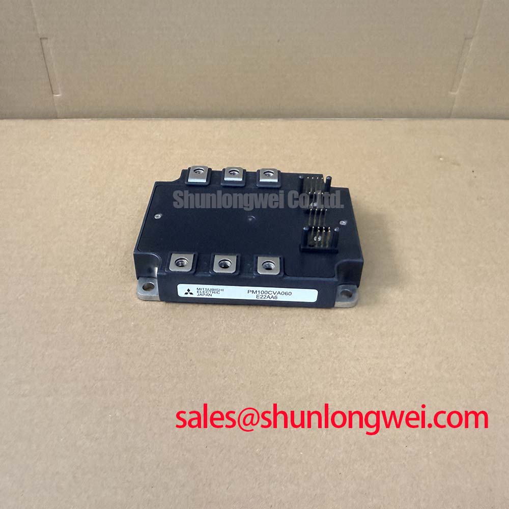
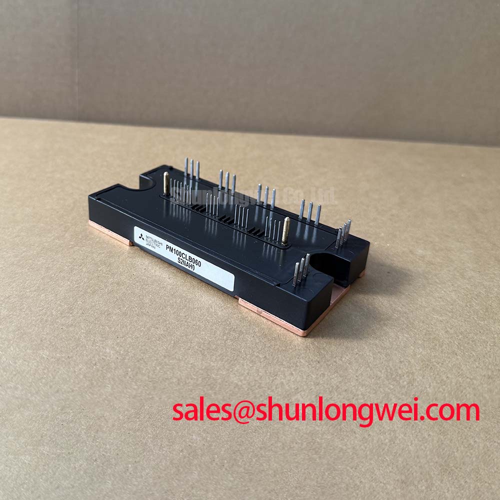
The PM100CL1A060 is a Mitsubishi Electric IPM module with a specified voltage rating of 600.0 V and a specified current rating of 100.0 A. These are official product parameters for initial replacement screening. Before installation in a heavy-duty variable frequency AC motor drive, compare the existing module’s electrical interface, protection behavior, mechanical arrangement, and thermal path with the equipment documentation.
| Manufacturer | Mitsubishi Electric |
| Part number | PM100CL1A060 |
| Product category | IPM Module |
| Specified voltage rating | 600.0 V, Official Specification |
| Specified current rating | 100.0 A, Official Specification |
| Package | Mitsubishi IPM Module, Official Product Classification |
For field replacement work, the voltage and current ratings establish the first screening boundary, not the complete operating envelope of the finished drive. The actual stress depends on DC-link behavior, switching conditions, motor cable construction, ambient temperature, cooling performance, gate-drive timing, and protection coordination. A system engineer should validate the installed module under the real load profile rather than treating the nameplate ratings as a complete drive design prescription.
Power-up shoot-through prevention starts with the sequence between the auxiliary gate-driver supply and the high-voltage DC link. The driver should reach its defined operating state, confirm UVLO interlocks, and establish the intended turn-off condition before the DC-link contactor or precharge path permits high voltage at the module terminals. If the auxiliary supply rises slowly, oscillates, or crosses its UVLO threshold repeatedly, the gate signal can become ambiguous during the same interval that the power stage is being energized.
A negative turn-off gate bias may be used as a system-level design consideration where the selected gate driver and module interface support it. Values such as −5 V to −15 V must be treated as an engineering range for driver evaluation, not as an official PM100CL1A060 module rating. The selected bias must remain within the original gate-drive documentation and must be checked for overshoot, isolation stress, common-mode transients, and compatibility with the protection circuit.
Use a controlled power-up test with the motor disconnected or with the approved low-energy commissioning arrangement. Monitor the auxiliary supply, UVLO status, high-side and low-side command signals, and gate-emitter voltage at the module terminals. A clean sequence should show that switching commands remain blocked while the driver is outside its valid supply window. If a gate waveform appears before the interlock is released, inspect the driver enable logic, optocoupler or digital isolator behavior, pull-down network, and return-current path.
Gate-loop layout requires a short, defined route between the driver output and the corresponding gate and emitter return. The power commutation path should not share a narrow control return with the gate-driver reference. This separation reduces the chance that common-mode ground bounce will be interpreted as a gate command. Designers should also minimize parasitic loop inductance and verify the resulting gate waveform at the module pins, rather than at a remote test point on the driver board.
MOV protection can be coordinated with the DC-link protection network as a design consideration. The MOV must be selected and placed according to the system’s repetitive energy, surge-current, leakage, and coordination requirements. It should not be treated as a substitute for correct gate sequencing or adequate semiconductor voltage margin. During commissioning, record the DC-link rise profile and switching-node behavior so that abnormal clamping activity can be distinguished from normal precharge operation.
Bench Diagnostic: Never connect or remove gate-drive wiring while the drive is energized; isolate the equipment, discharge stored energy, and confirm the absence of hazardous voltage with an approved measurement procedure.
Benchtop Waveform Tuning: Mitigating Stress via Long Motor Lead Reflected Wave Voltage on PM100CL1A060
Long motor leads can behave as a transmission-line system rather than a simple low-frequency cable, especially when fast inverter edges meet motor-end impedance discontinuities. Reflected energy can raise the voltage seen at the motor terminals and return stress to the inverter output stage. A commonly used engineering screening assumption is that a reflected-wave event can approach twice the local DC-link voltage at a terminal, but the actual peak depends on cable geometry, termination, switching speed, motor impedance, cable length, and measurement bandwidth.
For a heavy-duty variable frequency AC motor drive, begin waveform work with a properly rated differential probe and a measurement connection that does not introduce a long ground lead. Capture the output phase-to-phase and phase-to-ground waveforms at both the inverter and motor ends when practical. Compare the first overshoot, ringing frequency, repetition pattern, and damping behavior while changing operating frequency and load. An apparent spike may also be caused by probe resonance or an unsuitable reference connection, so the measurement arrangement must be checked before changing the hardware.
Output filters and chokes should be selected from the motor-drive topology, cable characteristics, carrier frequency, required common-mode performance, and thermal duty. A dv/dt filter can reduce edge steepness, while a sine-wave filter changes the waveform more extensively and may introduce additional voltage drop and reactive current. The appropriate network is determined by the complete drive and motor system; it should be validated for filter resonance, protection coordination, motor insulation stress, and the PM100CL1A060 switching behavior.
Short-circuit protection requires attention to desaturation sensing, blanking behavior, gate pull-down strength, and the soft turn-off sequence. A protection design may use a desaturation response target below 3 µs as an engineering objective, but this is not presented as an official PM100CL1A060 specification. The final timing must be established from the driver’s data and verified against the actual module, layout, measurement delay, and fault-current development.
Two-stage soft turn-off can be considered when an abrupt current interruption would create excessive collector-emitter overshoot. The first stage reduces the gate command in a controlled manner, while the second stage completes turn-off after the protection logic has recognized the fault condition. This approach must be coordinated with the driver’s fault latch and isolation delay. Excessive delay can increase short-circuit energy, while an overly aggressive turn-off can increase voltage overshoot through circuit inductance.
When tuning the waveform, evaluate the MOV, snubber, choke, and gate network as one transient system. The external Mitsubishi Electric SiC Power Modules and SBDs resource provides useful background on power semiconductor switching behavior, although its information should not be interpreted as a specification for this silicon IPM. The switching-node peak must be compared with the applicable module voltage boundary during controlled tests, with thermal and repetitive-stress effects included in the review.
For maintenance teams comparing available power-stage options, the CM10LD-12H may be reviewed as a separate power-stage candidate where its own voltage, current, gate interface, mechanical fit, and protection characteristics match the equipment documentation. It should not be installed as an automatic substitute without a complete interface and stress comparison.
PM100CL1A060 Thermal-Electrical Optimization: Thermal Stress Monitoring across High-Current Practical Tuning
At the specified current-rating level, terminal contact quality becomes part of the thermal design. A bolted joint with contamination, uneven pressure, damaged plating, or an unsuitable washer can create localized heating even when the module’s semiconductor junction remains within its expected electrical behavior. The first audit should be performed with the equipment isolated and the joint accessible, using a calibrated micro-ohmmeter and the same connection points for every comparison.
A contact-resistance value below 10 µΩ may be used as a project-specific inspection target when required by the equipment manufacturer or maintenance standard, but it is not identified here as an official PM100CL1A060 parameter. The measurement must exclude probe and fixture resistance, and the result should be compared with a known-good assembly or the approved service limit. A single resistance reading should not be used as the only acceptance criterion because clamping force, surface condition, temperature, and current distribution all influence the result.
Thermographic inspection should be performed after the drive has reached a repeatable operating condition. Capture the module terminals, busbar joints, cable lugs, heatsink interface, and neighboring phase connections using consistent emissivity settings and viewing angles. A warmer terminal does not automatically identify one failure mechanism; it may reflect unequal current sharing, a loose joint, busbar asymmetry, inadequate cooling, or a measurement artifact. Trace the temperature pattern back through the electrical and mechanical assembly before replacing the module.
Parallel-device arrangements require particular care with positive-temperature-coefficient behavior. When devices share current, small differences in conduction voltage, gate-loop impedance, emitter inductance, and thermal coupling can affect both static and dynamic current distribution. The external busbar should provide symmetrical electrical paths, while each gate-drive path should maintain consistent impedance and return routing. These are design considerations that require oscilloscope and thermal validation in the finished assembly, not assumptions based only on equal device ratings.
For continuous-load testing, log phase current, DC-link voltage, switching frequency, heatsink temperature, ambient temperature, and the temperature of each primary terminal. A useful maintenance comparison looks for changes between phases and changes from one service interval to the next. If one phase develops a different thermal profile, inspect its cable termination, busbar geometry, gate waveform, and current-sensor position before attributing the condition to the PM100CL1A060 itself.
The heatsink interface should be clean, flat within the equipment’s mechanical tolerance, and free from excessive thermal compound that could compromise seating. Mounting hardware should be tightened according to the drive manufacturer’s mechanical specification, with the module base supported evenly. Thermal interface material is a system assembly item rather than an independently confirmed module parameter, so its selection and application should follow the approved heatsink procedure.
Long-term evaluation can also include switching-loss trends, thermal imaging at multiple load points, and inspection of the gate waveform after thermal stabilization. The Wide Bandgap Revolution technical resource offers broader context on high-speed power semiconductor trade-offs; it does not replace the PM100CL1A060 electrical and mechanical documentation. Where a different semiconductor technology is considered, the gate-drive, protection, switching-frequency, and thermal assumptions must be recalculated for that device family.
When integrating the module into a replacement drive assembly, engineers should document the measured terminal condition, gate-driver sequence, transient waveform, and thermal image set as part of the equipment service record. This creates a practical baseline for later troubleshooting without assigning a single symptom to a single cause.