Content last revised on September 25, 2026
7MBP50TEA120 Electrical Design: Voltage Margin, Current Sharing, and Switching Checks
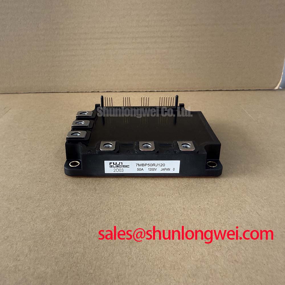
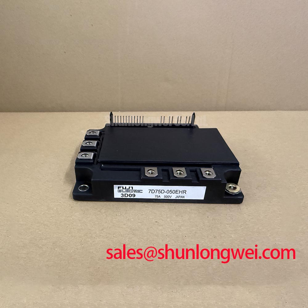
Before energizing a replacement unit, inspect the molded package and terminals, confirm the nameplate model, and record cold-state resistance and diode-test readings against a known-good reference. Keep the device unpowered and use ESD controls while checking the external power terminals, gate connections, and auxiliary interfaces. A multimeter reading alone cannot prove switching health, but it can reveal an open path, an unexpected short, or an obvious polarity mismatch before high-voltage testing.
The Fuji Electric 7MBP50TEA120 is a seven-pack intelligent power module combining an inverter stage, a brake stage, and an integrated drive section. Its specified collector-emitter voltage is 1200 V. The specified continuous collector current is 50 A at Tc = 80 °C, while the collector-emitter saturation voltage is listed as 2.3 V typical. These values establish the principal electrical identity of the part, but they do not represent a universal operating point for every inverter welder or medium-frequency induction heating supply.
| Parameter | Specified value | Engineering meaning |
|---|---|---|
| Collector-emitter voltage | 1200 V | Maximum voltage rating to be checked against the complete switching waveform |
| Continuous collector current | 50 A at Tc = 80 °C | Thermally conditional current capacity, not an unrestricted ambient rating |
| Collector-emitter saturation voltage | 2.3 V typical | Typical conduction reference requiring test-condition review |
| Module configuration | Seven-pack | Integrated inverter, brake, and drive arrangement |
| Thermal resistance | 0.44 °C/W per IGBT | Junction-to-case thermal reference for each IGBT |
| Integrated fault detection | OC, SC, OH, UV | Overcurrent, short-circuit, overheating, and under-voltage monitoring functions |
When the unit is evaluated in an industrial inverter welder, the first comparison should be between the original gate-drive timing, the DC-link voltage, and the measured collector-emitter waveform. Designers should verify turn-on and turn-off overshoot at the module terminals rather than relying on the nominal DC-link value. Parasitic inductance in the commutation loop can create a transient that is absent from a static voltage measurement. The system engineer should confirm peak voltage margin during switching tests with an appropriate differential probe and controlled current conditions.
For parallel current paths or multiple switching legs, symmetrical gate-loop routing is a practical design consideration. Keep power commutation conductors and gate-return conductors arranged consistently between equivalent positions. The positive temperature coefficient commonly associated with IGBT saturation voltage can assist static current sharing, but it does not remove the need to match gate impedance, propagation delay, emitter inductance, and physical loop area. Dynamic imbalance can still appear during fast transitions even when steady-state current appears similar.
The specified 2.3 V typical VCE(sat) should be used as a comparison point under its original test conditions. A higher measured value under load may reflect junction temperature, gate-drive amplitude, current level, probing location, or a change in switching timing. A lower reading under a different test condition should not be treated as proof of superior performance. Record collector current, case temperature, gate voltage, and measurement position with every comparison.
For a compatibility review, the neutral reference 7MBR50SB120-01 can be examined as a related module family reference. It should not be treated as an automatic substitute. Mechanical mounting, internal drive behavior, protection thresholds, terminal assignment, switching losses, and control-board timing must be checked against the equipment documentation before any interchange decision.
7MBP50TEA120 Thermal and Protection Evaluation for Practical Tuning
The published thermal reference for this module is Rth j-c = 0.44 °C/W per IGBT. This is a junction-to-case value, not a complete heatsink or enclosure thermal result. The final junction temperature depends on the interface condition, heatsink resistance, airflow, switching loss, conduction loss, duty cycle, and the temperature distribution across the baseplate. When evaluating a medium-frequency induction heating power supply, measure case temperature at a repeatable location and correlate it with electrical loading rather than inferring junction temperature from enclosure temperature alone.
The integrated protection suite includes overcurrent, short circuit, overheating, and under-voltage detection. Protection indicates that the module contains monitoring functions; it does not establish the trip delay, threshold tolerance, fault-reset sequence, or immunity to every external disturbance. The system integrator should obtain the relevant control and protection timing information from the applicable manufacturer documentation and then confirm that the host controller responds correctly to each fault state.
A practical incoming inspection begins with a visual check for cracked molding, bent terminals, contamination, and mechanical stress around the mounting area. With the module isolated from all external circuitry, use the diode function to compare corresponding freewheel paths and record polarity consistently. The expected result is not a universal single voltage value because the reading depends on the internal semiconductor path, meter current, temperature, and the terminals selected. An asymmetric result may justify a second measurement with reversed leads and a comparison to a known-good unit, but it should not be assigned a failure cause without further testing.
For gate-drive evaluation, check the command signal at the module interface and then at the gate-emitter terminals under the actual wiring arrangement. A clean controller-side pulse does not prove that the gate terminal receives the same waveform. Gate-loop inductance, shared returns, probe ground errors, and common-mode movement can distort the observed signal. Designers should minimize the gate-loop area and keep high-current commutation paths physically separated from sensitive control wiring, then verify the result with suitably rated isolated measurement equipment.
Claims concerning reinforced isolation voltage or common-mode transient immunity require a device-specific source. The supplied product data identifies the protection functions but does not provide a verified isolation withstand value or a CMTI specification for this model. Those properties should therefore be confirmed from the correct Fuji Electric documentation and the complete power-stack design. The external circuit should be tested for false gate triggering during the fastest expected switching event, with the DC-link and load conditions documented.
Phase-angle control, line-frequency ripple smoothing, and RC snubbers are system-level matters. An RC network can reduce ringing when its resistance, capacitance, physical placement, and pulse-energy capability match the measured parasitic network. It should not be added solely from a generic component value. Observe the voltage and current together, identify the ringing frequency and damping behavior, and verify that the snubber itself does not create excessive continuous loss. The same procedure applies when evaluating the brake path inside the seven-pack configuration.
Bench Tip: Keep the module in an ESD-controlled, de-energized state and compare cold measurements with a documented reference unit before applying the DC link.
Assembly Integrity and Layout Architecture for DC-Link Transients
Long motor leads, busbar transitions, and poorly positioned measurement points can produce terminal spikes that are substantially higher than the nominal DC-link voltage. A commonly discussed two-times-DC-link condition is a system-level transient possibility, not a published rating or guaranteed behavior of the 7MBP50TEA120. The correct assessment requires measuring the module terminals at the switching edge and considering cable impedance, motor characteristics, bus structure, clamp behavior, and probe bandwidth.
For an industrial inverter welder, place the high-frequency commutation path as a compact loop that includes the DC-link capacitor connection, module power terminals, and the return path. The layout objective is to reduce stray inductance and prevent the high di/dt current from sharing conductors with gate or fault-sense wiring. Clearance and creepage must be selected according to the working voltage, pollution environment, insulation system, and applicable equipment standard. No single clearance value can be assigned to this module without those system conditions.
When an induction-heating supply uses long output conductors, designers should evaluate the complete cable and load network before selecting an output filter or choke. The filter must be checked for voltage stress, current capability, resonance, acoustic behavior, and interaction with the control loop. A choke that reduces one ringing mode can shift energy into another frequency range. Use oscilloscope measurements at the module, filter input, filter output, and load connection to distinguish a switching-node transient from a cable-end reflection.
Mechanical assembly also affects electrical reliability. The mounting surface should be clean and flat, and the thermal interface should be applied consistently according to the equipment assembly specification. Uneven fastening can increase thermal resistance or stress the module base. The user’s maintenance procedure should define the approved fastener, tightening sequence, torque, and any recheck requirement; these values are not included in the supplied 7MBP50TEA120 electrical data.
Terminal identification must be checked against the original equipment drawing rather than inferred from physical proximity. The seven-pack arrangement contains multiple power and drive functions, so a harness that appears mechanically compatible can still place a control or auxiliary connection on the wrong node. Photograph the installed wiring before removal, record conductor destinations, and verify continuity with the DC link fully discharged. The integrated OC, SC, OH, and UV functions also require confirmation at the control connector so that a protective shutdown is not misinterpreted as a power semiconductor failure.
Where a replacement board uses separate power and signal returns, preserve that separation during service work. Do not extend a gate or fault conductor beside a high-current switching conductor merely to simplify cable routing. After assembly, perform low-voltage control checks first, then a restricted-energy switching test, and finally the intended load test while recording gate waveforms, collector-emitter voltage, current, and case temperature.
The article The Advanced Thermal Management Revolution provides a broader reference for thermal path evaluation, including the relationship between substrate construction, interface quality, and cooling architecture. It should support engineering review rather than replace the module-specific mounting and thermal requirements.
Transient Thermal Impedance and Pulsed Overload Verification
The continuous current specification of 50 A at Tc = 80 °C cannot be converted directly into a safe pulsed-current limit. Pulsed overload behavior depends on pulse width, repetition rate, starting junction temperature, conduction loss, switching loss, cooling path, and the manufacturer’s transient thermal impedance data. The term ITSM is normally associated with surge current ratings for thyristors and is not provided as a rating for this IGBT module. Engineers should therefore avoid importing an ITSM value from another semiconductor family.
For a short overload, the junction temperature rises according to the thermal impedance of the IGBT and the duration of the pulse. A multi-RC thermal model may be used as an engineering calculation when the model coefficients come from an authoritative thermal impedance curve or validated measurement. Without those coefficients, the supplied steady-state value of 0.44 °C/W per IGBT is insufficient to calculate a credible peak junction temperature for a particular pulse.
A useful test sequence begins by establishing the initial case temperature and the no-load switching waveform. Apply a controlled load pulse within the host system’s protective limits, capture collector current and collector-emitter voltage, and calculate instantaneous semiconductor power from synchronized voltage and current measurements. Repeat the test at the intended repetition rate because a single isolated pulse can produce a different thermal response from a burst or sustained duty cycle.
When the measured VCE(sat) changes during a pulse, interpret the result with the gate voltage and junction-temperature trend. Saturation voltage is influenced by current, temperature, gate-drive condition, and measurement connection. A rising value may warrant inspection of gate supply stability, emitter-return impedance, thermal interface quality, and load distribution. It does not independently identify a damaged die or a particular protection event.
Thermal recovery between pulses should be evaluated at the actual repetition frequency. A case that appears acceptable after one pulse may continue accumulating heat when the cooling system cannot remove the average loss. Designers should verify peak junction-temperature margin against the applicable manufacturer curves and the equipment shutdown limits. Where those curves are unavailable, limit testing to conditions supported by the equipment design and avoid presenting a calculated lifetime or overload capability as a product specification.
The Fuji Electric power semiconductor and IPM module resources are an appropriate starting point for locating manufacturer-level information about module operation and protection. The final acceptance procedure should still use the documentation matched to the exact part marking and equipment revision.
During fault investigation, capture the sequence of gate command, protection indication, current collapse, and DC-link behavior. The 7MBP50TEA120 includes OC, SC, OH, and UV detection, but the external controller determines how those signals are latched, delayed, displayed, and reset. Reviewing that complete sequence helps separate a thermal event, a supply undervoltage event, a short-circuit response, and a wiring or measurement problem without assigning a single cause from one static meter reading.