Content last revised on July 5, 2026
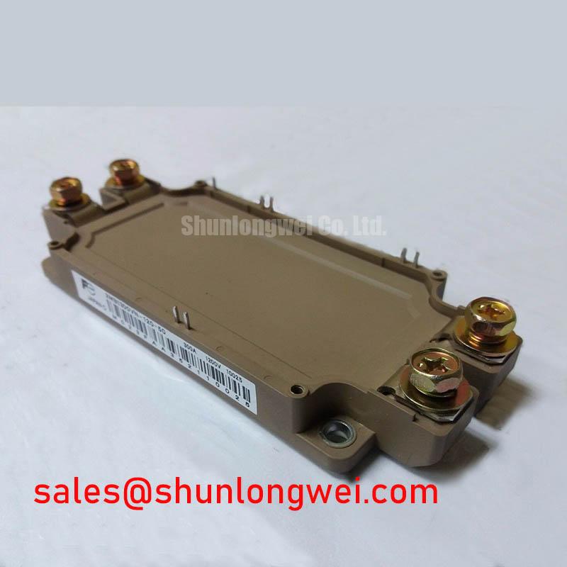
7MBR100U4B120-54: Fuji Electric 1200V 100A 7-in-1 Power Integrated Module (PIM)
Introduction to a Compact Powerhouse for Motor Control
The Fuji Electric 7MBR100U4B120-54 is a highly integrated Power Integrated Module (PIM) engineered to streamline the design of compact and efficient motor drive systems. This module consolidates a complete three-phase power stage into a single component, featuring key specifications of 1200V and 100A. Key engineering benefits include a significant reduction in system complexity and enhanced thermal monitoring capabilities. It directly addresses the need for a compact power solution with integrated rectification and braking, common in high-performance servo and inverter applications. For mid-range industrial drives requiring a robust, all-in-one power solution, this 7-in-1 PIM is an optimal choice for accelerating development and improving reliability.
Application Scenarios & Value
Achieving Power Density and Reliability in Industrial Automation
The 7MBR100U4B120-54 is engineered for applications where space, assembly efficiency, and operational reliability are critical design constraints. Its primary value is realized in systems such as compact Variable Frequency Drives (VFDs), precision servo drives for robotics and CNC machinery, and general-purpose industrial inverters up to approximately 45 kW. Consider an engineer designing a servo drive for a multi-axis automated assembly line. The primary challenge is fitting a complete power stage—including input rectification, a dynamic brake for deceleration, and the three-phase inverter—into a confined control cabinet. The 7-in-1 topology of this module directly solves this by integrating all seven power devices into one footprint, drastically simplifying the PCB layout and reducing assembly time. The module's 100A current rating provides ample capability for demanding motor acceleration and load profiles, ensuring precise control and robust performance. For systems requiring higher power output, the related 7MBR150VR120 provides a similar integrated topology with a higher current capacity.
Key Parameter Overview
Decoding the Specs for Integrated Drive Design
The technical specifications of the 7MBR100U4B120-54 are optimized for balanced performance in motor control applications. The parameters are organized below by their function within the module to provide clarity for system designers. What is the benefit of its 7-in-1 integration? It simplifies design, reduces assembly costs, and minimizes stray inductance.
| Parameter | Value | Notes |
|---|---|---|
| Absolute Maximum Ratings (Tc=25°C unless otherwise specified) | ||
| Collector-Emitter Voltage (Vces) | 1200V | Applies to Inverter and Brake IGBT sections. |
| Gate-Emitter Voltage (Vges) | ±20V | Maximum allowable gate drive voltage. |
| Continuous Collector Current (Ic) | 100A (Tc=80°C) | Defines the continuous current handling for the inverter section. |
| Repetitive Peak Reverse Voltage (VRRM) | 1200V | For the three-phase rectifier diode section. |
| Operating Junction Temperature (Tj) | +150°C | Maximum operational temperature for the semiconductor junctions. |
| Electrical Characteristics (Tj=25°C) | ||
| Collector-Emitter Saturation Voltage (Vce(sat)) | 1.80V (typ) / 2.35V (max) | At rated current (Ic=100A), indicating low conduction losses. |
| Forward Voltage (VF) - FWD | 1.75V (typ) | For the freewheeling diodes in the inverter section. |
| NTC Thermistor Resistance (R25) | 5 kΩ | Resistance at 25°C for temperature sensing. |
Application Vignette
Enhancing Reliability in a Compact CNC Spindle Drive
A significant challenge in designing drives for modern CNC spindles is managing thermal performance within a progressively shrinking footprint. The drive must handle rapid acceleration and deceleration cycles, which generates substantial heat. The 7MBR100U4B120-54 provides a direct engineering solution. Its low Thermal Resistance ensures efficient heat transfer from the silicon to the heatsink. More critically, the integrated NTC thermistor offers a precise way to monitor the module's substrate temperature in real-time. This allows the drive's controller to implement intelligent thermal management strategies, such as derating the output current or increasing fan speed before a critical over-temperature fault occurs. Think of the NTC thermistor as a built-in early warning system, preventing catastrophic failure and extending the operational life of both the drive and the motor. This integrated feedback loop is a key enabler for building reliable, high-duty-cycle power systems, a core requirement in advanced industrial automation and manufacturing equipment.
Frequently Asked Questions
What is the primary benefit of the integrated NTC thermistor in the 7MBR100U4B120-54?
The integrated NTC thermistor provides a direct, real-time measurement of the module's internal temperature. This allows for precise over-temperature protection and enables sophisticated thermal management within the drive's control system, leading to enhanced system reliability and longevity.
How does the 7-in-1 topology of the 7MBR100U4B120-54 simplify motor drive design?
By integrating the three-phase input rectifier, brake chopper, and three-phase output inverter into a single package, it eliminates the need for multiple discrete components. This significantly reduces the required PCB area, simplifies the assembly process, lowers manufacturing costs, and minimizes parasitic inductance between power stages, which can improve electrical performance.
For designers developing next-generation motor drives and power converters, the 7MBR100U4B120-54 offers a compelling combination of integration, performance, and built-in thermal protection. To fully assess its suitability for your specific design requirements, a thorough review of the official datasheet is recommended to understand its dynamic characteristics and safe operating areas. Our technical team is available to provide further information to support your engineering evaluation.