
Content last revised on September 10, 2026
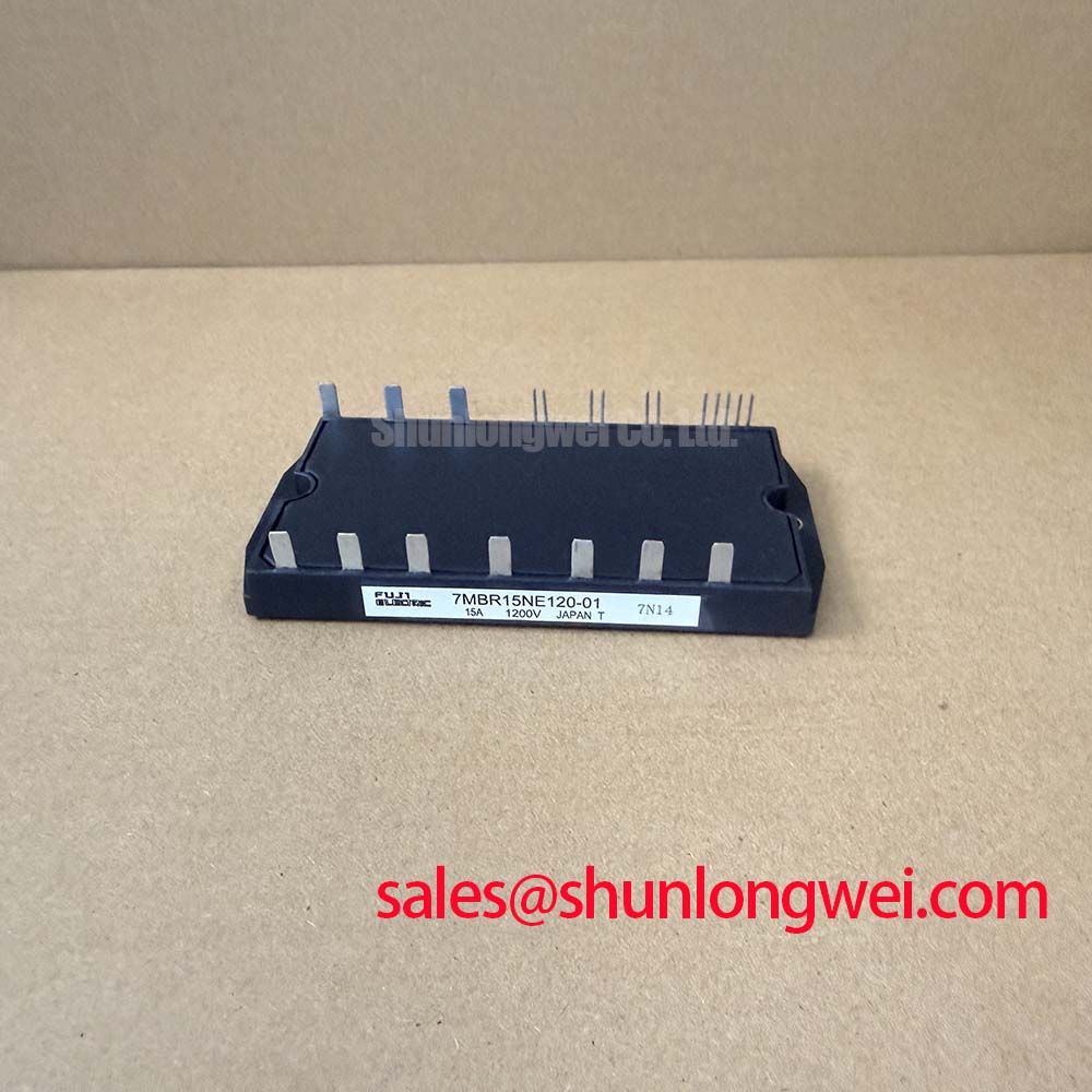
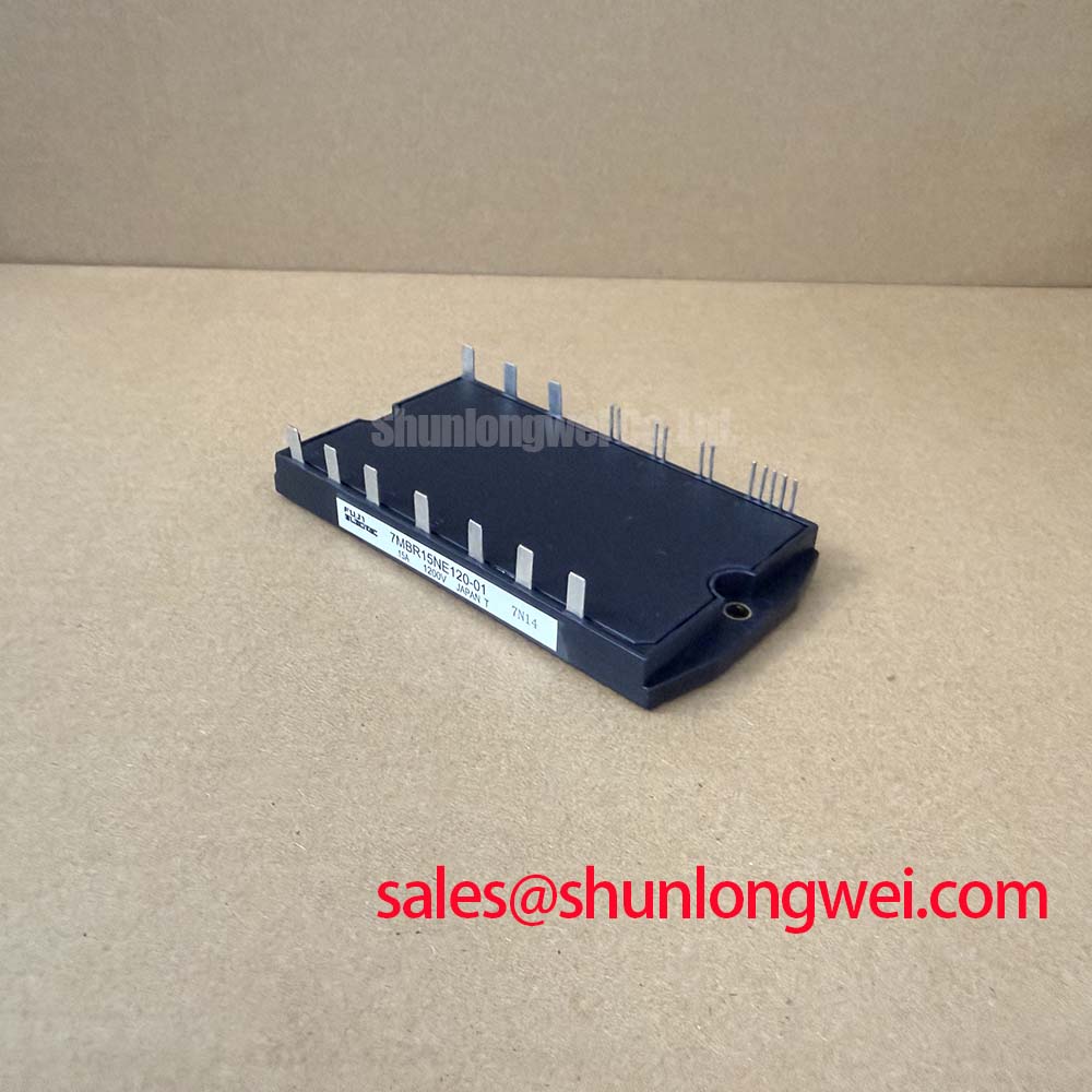
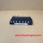
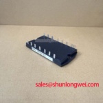
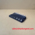
Initial bench inspection of the 7MBR15NE120-01 power module begins with a static polarity and diode forward voltage verification across all terminal pairs using a calibrated digital multimeter in diode-test mode. Cold junction continuity checks establish baseline health before applying DC bus potentials, confirming that internal bridge rectifiers, the dynamic brake circuit, and the three-phase inverter stage show no latent open-circuit anomalies or gate-to-emitter punch-through defects. Measuring pin impedances under static conditions prevents catastrophic flashovers when retrofitting high-precision robotic servo wrist actuators or multi-joint motion controllers.
7MBR15NE120-01 Circuit Protection & Reliability: Calibrating Overvoltage Trip Prevention via Fast-Switching Dynamic Braking
Static verification of the integrated dynamic brake arm begins by testing the collector-to-emitter path of the chopper IGBT and its accompanying antiparallel clamp diode. The 7MBR15NE120-01 integrates a dedicated internal brake stage rated at VCES(Brake) = 1200 V (Official Datasheet Specification). When decelerating high-inertia kinetic loads in industrial robotics, counter-electromotive force (CEMF) feeds back through the inverter freewheeling diodes into the shared DC bus. If this energy is not dissipated, the intermediate link voltage quickly exceeds the continuous rating of the smoothing electrolytic capacitor bank, triggering an overvoltage fault trip.
To safely evaluate the dynamic braking circuit on the test bench, technicians connect a dummy load bank across the brake collector and external DC bus positive rail. The input rectifier stage handles incoming three-phase AC with a maximum repetitive peak reverse voltage of VRRM = 1600 V (Official Datasheet Specification), converting line energy into an intermediate DC level that typically sits between 540 V and 680 V under nominal 400/480 VAC industrial mains. During sharp motor deceleration profiles, dynamic bus voltage monitoring threshold switches the internal brake IGBT into conduction at an engineered trigger point (typically 750 V DC as an Engineering Recommendation).
Proper ballast resistor sizing prevents the brake IGBT from exceeding its pulsed energy absorption boundaries. Integrating engineers must coordinate the thermal mass of the ballast resistor with the transient thermal impedance network of the module. When cross-referencing legacy installations or alternative layout revisions, designers frequently cross-reference modules like the 7MBR15SA120 to establish braking dissipation parallels across equivalent package profiles.
| Sub-Circuit Stage | Parameter Symbol | Technical Specification Parameter | Official Rating & Parameter Class |
|---|---|---|---|
| Inverter Stage (IGBT) | VCES | Collector-Emitter Breakdown Voltage | 1200 V (Official Datasheet Specification) |
| Brake Chopper Stage | VCES(Brake) | Brake Collector-Emitter Breakdown Voltage | 1200 V (Official Datasheet Specification) |
| Input Rectifier Stage | VRRM | Repetitive Peak Reverse Voltage | 1600 V (Official Datasheet Specification) |
| Module Isolation | Viso | AC Isolation Voltage (Terminals to Baseplate, 1 min) | 2500 V AC (Official Datasheet Specification) |
| Thermal Limits | Tj / Tstg | Operating Junction / Storage Temperature | -40 to +150 °C / -40 to +125 °C (Official Datasheet Specification) |
Assembly Integrity & Layout Architecture: Implementing High dv/dt Cross-Conduction Shoot-Through Prevention for 7MBR15NE120-01
High switching speeds inside compact Power Integrated Modules (PIM) expose gate control loops to displacement currents triggered by steep phase-node voltage gradients. In the six-pack inverter section of the 7MBR15NE120-01, collector-emitter switching transients generate capacitive displacement currents through the Miller capacitance (Cres or Cgc). When a high-side IGBT turns on rapidly, the complementary low-side device experiences a rapid rise in collector potential (dv/dt), forcing current through its internal collector-gate capacitance into the gate impedance network.
Without adequate low-impedance grounding, this parasitic displacement current raises the low-side gate voltage above its threshold conduction level (VGE(th)), inducing momentary bridge shoot-through. To eliminate false parasitic turn-on, driver circuitry should implement an active Miller clamp or a true negative off-state bias voltage between -5 V and -15 V (Design Consideration for noisy industrial environments). An active Miller clamp monitors the gate node during turn-off; once the gate voltage drops below approximately 2.0 V, a low-impedance bipolar transistor or MOSFET shorts the gate directly to the emitter rail, bypassing the external turn-off series resistance.
Selecting the external gate resistance (Rg) requires balancing dynamic switching losses with transient voltage spikes. A gate resistor that is too small promotes severe high-frequency oscillation, whereas excessive damping increases turn-on switching loss (Eon) and turn-off switching loss (Eoff). For multi-axis robotic drive platforms where power density is critical, gate circuit traces must remain tightly coupled and routed as short twisted pairs or direct differential planar PCB layers to prevent magnetic induction from adjacent high-current inverter phases. For higher-power distribution stages feeding auxiliary automation lines, system designers routinely study larger complementary modules such as the 7MBR50SB120-01 to determine appropriate scaling factors for gate charge and damping resistance.
💡 Bench Tip: Maintain an ESD-grounded conductive wrist strap during any impedance or gate-charge test; verify cold-state gate-to-emitter leakage with an electrometer before gate-driver assembly, ensuring leakage stays below 100 nA at 20 V bias to rule out handling-induced gate oxide puncturing.
Transient Dynamics & Electrical Design: High-Frequency Commutation Loop Inductance on 7MBR15NE120-01
During turn-off transitions, the rate of current decay (di/dt) across the IGBT combined with stray parasitic inductance creates an instantaneous overvoltage stress on the silicon die. The peak transient voltage is governed by the relation where the total peak collector-emitter potential equals the continuous DC link voltage plus the inductive induced spike: Vpeak = VDC + L_sigma * (di/dt). If total commutation loop inductance (L_sigma) is uncontrolled, this inductive kick can exceed the rated VCES = 1200 V (Official Datasheet Specification), causing immediate avalanche puncture.
Minimizing parasitic loop inductance requires a disciplined layout architecture between the module terminal pins, the DC link smoothing bus, and the local decoupling snubber. Integrating ultra-low Equivalent Series Inductance (ESL) film capacitors directly across the P and N terminals reduces the effective commutation loop length. Stacking the positive and negative planar bus conductors with thin insulation creates mutual flux cancellation, achieving target loop inductance figures well below 25 nH (General Industry Design Consideration).
When running load cycling evaluations, engineers assess the reverse recovery softness factor (S-factor) of the integrated freewheeling diodes. A snap-off recovery characteristic produces severe high-frequency ringing in the 30 MHz to 100 MHz spectrum, which propagates through motor cabling and stresses ground insulation. Soft-recovery freewheel diodes mitigate electromagnetic radiation and dampen the inductive overshoot across the inverter bridge. Structural thermal and electrical design standards detailed within the Industrial Applications research papers emphasize matching DC link decoupling network parameters to module internal bond-wire physics to maximize switching life.
Baseline parameters can be cross-verified against official technical documentation via the Fuji Electric Power Semiconductors Portal. For advanced system retrofits requiring specialized wide-bandgap topologies, engineers can evaluate complementary technologies via the Fuji Electric Discrete IGBT & SiC MOSFETs technical database.
7MBR15NE120-01 Operational Boundaries: Evaluating Desaturation Detection Limits
Protecting the 7MBR15NE120-01 during severe downstream mechanical jams or phase-to-phase insulation breakdowns requires high-speed short-circuit fault handling. Under short-circuit conditions (Type-I short with fault initiation before turn-on, or Type-II short occurring mid-conduction), current through the IGBT escalates into desaturation within fractions of a microsecond. The device exits its low-loss saturation region and moves into active linear operation, leading to extreme internal thermal dissipation as the entire DC bus potential drops across the active channel.
To survive without silicon rupture, short-circuit faults must be detected, validated, and safely quenched within the Short-Circuit Safe Operating Area limit of tsc < 10 µs (Official Datasheet Specification boundary for standard industrial silicon). Desaturation detection circuits operate by continuously sampling the forward collector-emitter voltage via a high-voltage blocking diode while the gate drive signal is commanded high. A blanking capacitor delays measurement for 1.5 µs to 3.0 µs immediately following turn-on, preventing false fault latching caused by the finite forward recovery time of the IGBT.
Once VCE exceeds the set threshold (typically 6.5 V to 8.0 V based on drive circuit component tolerances), the controller initiates an automated two-stage soft turn-off (Soft Shut-Down, SSD). Abruptly clamping the gate voltage to ground during a short-circuit event produces an extreme di/dt condition that triggers an immediate overvoltage breakdown due to trapped energy in stray parasitic inductances. A two-stage soft shut-down introduces a controlled high-resistance discharge path, slowly ramping down gate charge over several microseconds to discharge channel current safely within the safe electrical and thermal boundaries of the package.
⚡ Safety Interlock Note: Always torque module mounting screws in two stages to a final value of 2.5 to 3.5 N·m using an alternating diagonal sequence to prevent localized ceramic substrate cracking and preserve the 2500 V AC isolation rating.
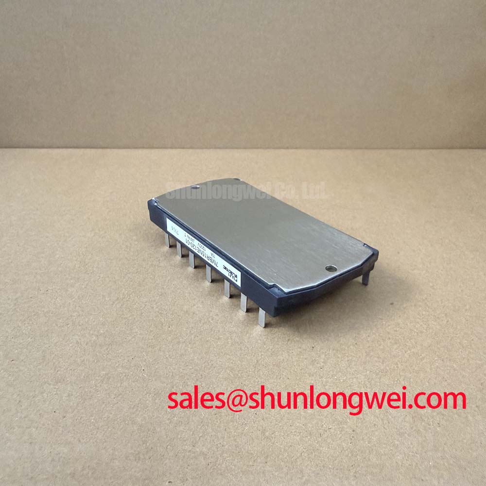
Verification on the incoming QA test bench concludes by confirming the galvanic isolation barrier between all internal circuit terminals and the thermally conductive baseplate. Applying Viso = 2500 V AC for 60 seconds (Official Datasheet Specification) while monitoring leakage current ensures the internal DCB (Direct Copper Bonded) ceramic substrate is free of micro-fractures, voids, or mechanical assembly stress before installation into production machinery.