Content last revised on September 10, 2026
Preventing Spurious Faults: Fault-Clearing Dynamics for Fuji Electric 7MBR30SC060
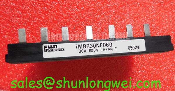
Begin a replacement inspection by checking the Fuji Electric marking, confirming the 600 V rated voltage and 30 A rated current against the equipment documentation, then examining the module body, terminals, and mounting surface before energizing the circuit. These are the available official product specifications for the 7MBR30SC060; gate timing, short circuit withstand capability, isolation ratings, and internal topology should be confirmed against the applicable Fuji Electric datasheet before a protection scheme is finalized.
For a PIM used in a light industrial automation drive or multi-joint robotic articulator, desaturation protection is a system-level design consideration rather than an automatically confirmed feature of this specific module. If the module documentation supports desat monitoring, the protection circuit should distinguish a genuine overcurrent event from noise coupled into the sensing path. A fast fault-recognition approach can provide rapid protection, while filtering or a staged response may be used when the system requires additional noise immunity. A sub-10 µs clearing objective may be evaluated during development, but it must remain an engineering target validated against the applicable datasheet data and the actual gate driver response.
Two-stage soft turn-off is commonly evaluated where an abrupt gate discharge could produce excessive inductive voltage. The first stage reduces collector current in a controlled manner; the second stage completes shutdown after the driver has confirmed the fault condition. The correct timing, gate voltage, and discharge current are system-determined. Engineers should verify the collector-emitter overshoot with a properly referenced oscilloscope probe during short-circuit and abnormal-load testing, rather than relying only on the driver fault flag.
Keep the desaturation return path separate from high-current commutation conductors, minimize the sensing loop area, and provide adequate creepage and clearance for the working voltage of the complete assembly. If a nuisance fault appears, compare the fault waveform with a known-good phase, inspect the blanking and filtering network, and check whether the gate-emitter signal is being disturbed by common-source or power-loop inductance. The Fuji Electric Power Semiconductor and IPM Modules resource is useful for understanding the manufacturer’s broader module product context, but the exact protection behavior remains part-number specific.
Transient Dynamics and Electrical Design: Derating and Parameter Matching
The 7MBR30SC060 is specified as a 600 V, 30 A Module. Those ratings identify the component’s nominal electrical class, not a universal operating point for every inverter, servo amplifier, or robotic axis. The system designer should evaluate bus voltage, switching frequency, load profile, cooling conditions, fault exposure, and repetitive switching transients before applying a derating policy. Any safe operating area, junction temperature, surge-current, or short-circuit limit must be taken from the relevant manufacturer documentation.
Positive temperature behavior of on-state voltage can support static current sharing in matched parallel semiconductor paths, because a warmer path may develop a higher on-state voltage and naturally discourage unlimited current concentration. This principle does not guarantee dynamic sharing. Gate wiring must be electrically symmetrical, with comparable conductor length, return impedance, driver strength, and local decoupling. If current imbalance is suspected, measure each gate-emitter waveform and compare collector-current timing under the same load condition.
Gate-driver sourcing and sinking capability should be selected from the required switching speed, total gate charge, driver isolation arrangement, and permissible overshoot. An external gate resistor is a tuning component, not a fixed specification of the module. A practical engineering recommendation is to begin with the value used by the proven reference design, then adjust it while monitoring ringing, switching loss, gate voltage margin, and electromagnetic coupling. The final value should be determined through double-pulse or representative motor-load testing.
MOVs and other clamping networks should be coordinated with the DC-link capacitor, stray inductance, braking path, and the module’s verified voltage limits. A MOV selected only by nominal voltage can conduct too early, age under repetitive energy, or fail to control the highest-energy transient. The protection network should therefore be evaluated for clamping level, pulse energy, repetition rate, and thermal recovery. When a higher-current sibling is being assessed, the 7MBR50LC060 can be reviewed as a separate product record; its suitability cannot be inferred solely from the shared product-family naming.
Benchtop Waveform Tuning: Thermal Interface Control and Assembly Verification
Thermal measurements should start with a clean, flat mounting surface and a controlled thermal interface. Apply a continuous, thin layer of suitable thermal compound without trapped air pockets, then inspect the contact pattern after a controlled trial assembly. The objective is consistent heat transfer across the module baseplate. Excess compound can increase thermal resistance and contaminate nearby insulation, while insufficient coverage can leave localized dry regions.
Baseplate curvature or uneven hardware loading can create a contact pattern that looks acceptable at the screw heads but remains poor beneath the center of the module. Use the equipment manufacturer’s mounting sequence and torque information when available. If that information is unavailable, the fastening method should be treated as a Design Consideration and validated with the actual heatsink, interface material, and baseplate geometry. Tighten progressively in a cross-pattern so the module is not pulled toward one corner.
Thermal-electrical correlation is important during waveform tuning. Record heatsink temperature, case temperature where accessible, phase current, gate voltage, and switching-node overshoot together. A waveform that appears electrically clean at room temperature can change as the thermal interface reaches steady state. If the temperature rise is unexpected, inspect mounting flatness, compound distribution, airflow, sensor placement, and load balance before attributing the issue to the semiconductor itself.
In a bidirectional DC-DC battery charger or regenerative axis, repeated charge and discharge transitions can produce thermal cycling. The module’s suitability for that duty must be checked against its published thermal impedance, junction-temperature limits, power-cycle capability, and the converter’s measured loss profile. No field lifetime figure should be assigned without an authoritative test method and application-specific data. The related IGBT Design and Integration reference can support broader evaluation of gate-drive, thermal-management, and circuit-topology decisions.
Safety Interlock Note: Isolate the DC link and verify discharge before touching the module terminals, gate wiring, or oscilloscope connections.
7MBR30SC060 Thermal-Electrical Optimization: Transmission-Line Mismatch and Practical Tuning
Long motor leads can behave as a transmission-line system, especially when the inverter switching edge is fast compared with the cable propagation and reflection behavior. A reflected wave may raise the motor-terminal voltage substantially above the local inverter waveform; the actual peak depends on DC-link voltage, cable length, termination, motor impedance, switching speed, and measurement position. The frequently cited possibility of a terminal spike approaching twice the incident bus-related step is a Design Consideration, not a guaranteed behavior of the 7MBR30SC060.
Measure both the module-side switching node and the motor terminals with suitable high-voltage differential probes. Probe grounding, bandwidth, loop area, and common-mode rejection can materially alter the displayed waveform. Compare the result at several operating currents and switching conditions. If the motor-end overshoot is excessive, the system integrator should evaluate output reactors, dv/dt filters, sinusoidal filters, cable selection, switching-edge adjustment, and motor insulation limits as a coordinated network.
Filter and choke sizing must be based on the converter’s current waveform, carrier behavior, motor impedance, allowable voltage rise, thermal loss, and resonance risk. A filter that reduces edge speed may also increase semiconductor switching loss or interact with the cable capacitance. Validate the final arrangement with temperature measurements, conducted-noise checks, motor-terminal voltage measurements, and fault-protection tests.
Where the DC link includes a front-end rectifier or a related regenerative topology, the 7MBR50SB120-01 may be reviewed as a separate complementary-stage device. Its electrical role and ratings must be verified independently. Likewise, thyristor gate requirements such as IGT, VGT, pulse strength, and pulse-train behavior belong to the selected thyristor and its driver, not automatically to this Fuji Electric PIM. A battery system that combines these stages should validate commutation, surge-current recovery, thermal cycling, and control timing at the complete assembly level.