Content last revised on September 10, 2026
Fuji Electric 7MBR15SA120 Technical Overview & Field Engineering Specifications
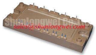
The 7MBR15SA120 is a Power Integrated Module (PIM) manufactured by Fuji Electric, integrating a three-phase input bridge rectifier, a three-phase output inverter stage, a dedicated dynamic brake chopper, and an integrated NTC thermistor inside a single compact housing. Designed with an industry-standard 7-pack configuration, this module provides compact power conversion for auxiliary power stages, precision servo amplifiers, and sub-inverter stages within utility-scale solar installations and industrial plant infrastructure.
Operating with a rated collector-emitter voltage of 1200V (Official Datasheet Specification) and a continuous collector current rating of 15A at 25°C (Official Datasheet Specification), the module balances low conduction losses with optimized switching speed. With a typical saturation voltage of VCE(sat) = 2.1V (Official Datasheet Specification) and an electrical isolation capability of 2500V AC for 1 minute (Official Datasheet Specification), the assembly maintains dependable electrical clearance and operational stability under heavy cycling profiles.
| Parameter Item | Technical Specification | Engineering Value / Condition |
|---|---|---|
| Manufacturer | Fuji Electric | Industrial Power Semiconductor Line |
| Model Number | 7MBR15SA120 | Integrated 7-Pack PIM Configuration |
| Collector-Emitter Voltage (VCES) | 1200V | Official Datasheet Specification (Tj = 25°C) |
| Continuous Collector Current (IC) | 15A | Official Datasheet Specification (Tc = 80°C) |
| Saturation Voltage (VCE(sat)) | 2.1V (Typical) | Official Datasheet Specification (IC = 15A, VGE = 15V) |
| Circuit Topology | PIM / 7-Pack | Converter + Inverter + Dynamic Brake + NTC |
| Isolation Voltage (VISO) | 2500V AC | Official Datasheet Specification (1 Minute, Terminals to Baseplate) |
| Maximum Junction Temperature (Tj) | 150°C | Official Datasheet Specification (Continuous Operation) |
Thermal Paste Degradation Prevention and Mechanical Clamping Torque Calibration
In continuous-duty environments such as industrial motor drives and utility string inverter auxiliary stages, thermal interface management dictates the mean-time-between-failures (MTBF) of the power stage. The copper baseplate of the 7MBR15SA120 requires uniform contact across the aluminum heatsink to ensure low junction-to-case thermal resistance Rth(j-c). Applying non-curing thermal grease must be strictly controlled to a dry-film thickness between 50 μm and 100 μm (Design Consideration). Excessively thick paste layers introduce unnecessary thermal impedance, while insufficient application creates air pockets that lead to localized thermal hotspots during full-load dynamic transitions.
⚠️ Maintenance Note: During routine PM (Preventive Maintenance) plant turnarounds, inspect the thermal compound around the module perimeter for signs of "pump-out" or grease chalking caused by repetitive power thermal cycles. If baseline junction temperatures rise by more than 8°C under identical ambient and load conditions, the module should be dismounted, the old thermal compound cleaned with high-purity isopropyl alcohol, and fresh compound applied using a precision stencil or screed.
Mechanical mounting integrity demands strict adherence to screw fastening sequences. The heatsink surface flatness must remain within 50 μm per 100 mm span, with a surface roughness of Rz ≤ 10 μm (Design Consideration). When fastening the M5 mounting hardware, apply a progressive two-stage torque sequence: pre-tighten all screws diagonally to 1.0 N·m, followed by final torque calibration within the recommended range of 2.5 N·m to 3.5 N·m (Design Consideration). Imbalanced torque creates baseplate warping, stressing internal direct bonded copper (DBC) ceramic substrates and promoting micro-cracking across solder interfaces under sustained thermal cycling.
Symmetrical Busbar Geometry for High-Current Parallel Module Arrays
When engineering multi-channel power conversion systems or matching subsystem current ratings, balancing DC link connections is critical. For systems requiring higher continuous current handling in primary conversion blocks, the related 7MBI100U4E-120-50 provides a 100A, 1200V platform, whereas the 7MBR15SA120 serves low-to-medium power processing branches and dynamic braking channels. In three-phase topologies involving multiple discrete branches, asymmetrical busbar geometry introduces divergent loop inductances, driving unbalanced dynamic current sharing across parallel bridge legs.
Low-inductance planar busbar design principles must be implemented to keep DC-bus loop stray inductance Lσ to a minimum. During aggressive turn-off events, collector current fall rates (di/dt) interacting with parasitic trace inductance generate transient overvoltage spikes that stress the 1200V collector-emitter boundary. Incorporating low-ESR film snubber capacitors directly across the module's positive (P) and negative (N) terminals dampens inductive voltage peaks, clamping collector overshoot safely below 80% of rated VCES under emergency shutdown conditions.
Short-circuit protection requires fast desaturation detection circuits tuned specifically for the module's 2.1V typical VCE(sat) conduction baseline. The desaturation blanking time should be calibrated to less than 3.0 μs (Design Consideration) to prevent nuisance tripping during initial turn-on while guaranteeing two-stage soft turn-off execution within the module's short-circuit withstand rating. The positive temperature coefficient exhibited by the silicon at rated currents aids static current sharing, yet dynamic balancing remains entirely dependent on strict symmetrical trace length routing from the DC link decoupling bank.
Dynamic Gate Impedance Control for Robust Phase-Leg Dead-Time Operation
Phase-leg commutation reliability in compact PIM architectures requires balancing switching loss dissipation against electromagnetic emissions and parasitic gate bounce. With integrated six-switch inverter stages alongside a dedicated chopper transistor, gate signal integrity is vulnerable to rapid dv/dt transients generated during complementary device switching. To verify root-cause failure mechanisms and proper driver signal integrity, plant technicians should cross-reference standard diagnostic procedures outlined in the Field Engineer’s Handbook for gate-drive waveforms and thermal mapping protocols.
To eliminate parasitic turn-on induced by displacement currents flowing through the Miller capacitance (Cres), field designs should adopt an active Miller clamp circuit or provide a dedicated negative gate bias voltage between -5V and -15V (Design Consideration). When single-supply gate drivers (0V / +15V) are deployed without negative bias, high dVCE/dt across the adjacent collector-emitter junction forces capacitive current into the gate circuit. If this current exceeds the pull-down sink capability of the gate driver, gate potential rises above the threshold voltage VGE(th), causing catastrophic shoot-through cross-conduction across the DC rail.
Selecting the external gate resistance RG requires careful empirical validation. A suggested initial gate damping value of RG(on) / RG(off) = 33 Ω to 68 Ω (Typical Starting Point for bench tuning) allows field technicians to balance turn-on di/dt against turn-off switching energy Eoff. For secondary rectifier integration and front-end isolation stages, complementary modules such as the 6MBI10S-120 illustrate similar gate-drive impedance matching strategies across six-pack configurations. Dead-time settings for the pulse-width modulation (PWM) controller must be programmed with a minimum deadband of 1.5 μs to 2.5 μs (Design Consideration) to prevent half-bridge cross-conduction across varying junction temperatures.
Cosmic Ray Robustness: Voltage Derating Curves across 2000m-4000m Altitudes
Deploying power conversion equipment in high-altitude industrial areas or utility solar fields situated at 2000 to 4000 meters above sea level introduces severe environmental stress factors. Atmospheric pressure reductions diminish dielectric breakdown strength of air, requiring re-evaluation of external creepage and clearance distances in accordance with IEC 60664-1 standards. Concurrently, cooling fan volumetric efficiency drops, leading to an effective derating in heat exchanger thermal dissipation capacity.
At elevated altitudes, terrestrial cosmic ray neutron flux intensity increases significantly compared to sea-level baselines. High-energy atmospheric neutrons colliding with silicon lattice structures in the depletion region can trigger catastrophic Single Event Burnout (SEB) failures without prior thermal degradation. Because SEB susceptibility rises exponentially with continuous electric field stress, the steady-state operating DC bus voltage must be deliberately derated when configuring high-altitude power conversion stages.
For standard sea-level operation, a 1200V rated module commonly operates at an operational DC link voltage between 600V and 800V DC. However, when installed at altitudes exceeding 2000 meters, technical engineering design guidelines strongly recommend derating maximum continuous DC link voltage to 600V–650V DC (Design Consideration) to maintain acceptable FIT (Failures In Time) rates. Detailed platform specifications and mechanical outline diagrams can be examined via the official Fuji Electric PIM (Power Integrated Module) 7-Pack technical documentation, ensuring precise alignment with plant engineering enclosures and maintenance replacement standards.