

Content last revised on October 15, 2026
Transient Dynamics & Electrical Design: High-Speed Fault Management: VCE Desaturation on 7MBR50UA120
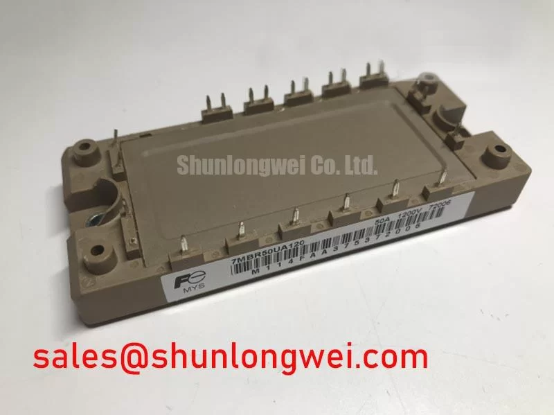
With the traction inverter isolated and the DC link fully discharged, first inspect the module terminals for discoloration, looseness, or heat-related distortion before applying any gate signal. Confirm the nameplate selection against the replacement record: Fuji Electric 7MBR50UA120 is specified at 1200.0 V and 50.0 A. These ratings identify the device; they do not replace the switching, thermal, and protection limits required by the complete drive design.
In a forklift traction inverter, a desaturation circuit should observe the collector-emitter condition during commanded turn-on and react to an abnormal rise in VCE. Type-I and Type-II short-circuit events can develop within a very short switching interval, so the protection chain should be evaluated for detection and gate-control response within the intended sub-cycle protection window. A design target such as detection within 10 µs belongs to the system protection specification and must not be treated as a factory rating of this module. The total detection and turn-off time must remain within the device’s documented short-circuit withstand capability under the applicable conditions.
The practical objective is to remove gate drive energy without creating a second damaging event. A two-stage soft turn-off sequence can first reduce the gate-emitter voltage and then complete controlled turn-off, limiting the voltage excursion caused by stray inductance and load current. The driver, desaturation diode, blanking network, isolation barrier, and gate-return path must be tested as one protection loop. A slow optocoupler or excessive propagation mismatch can leave the device exposed even when the protection threshold appears correct during a static bench check.
Keep the desaturation sensing loop physically separate from high-current commutation conductors. The return path should reference the intended emitter potential rather than a distant power ground, while the gate-driver supply bypass path should remain short and low impedance. Clearance around the high-voltage switching nodes must support the working voltage, pollution environment, board material, and enclosure conditions selected by the system engineer. Creepage and clearance are layout requirements, not characteristics that can be inferred from the 1200 V rating alone.
During troubleshooting, compare the gate-emitter waveform, desaturation-sense waveform, driver fault output, and collector-emitter voltage on the same time base. A fault that appears only under load may involve commutation inductance, current-sensor delay, driver saturation, or an unexpected freewheeling path. If the fault circuit trips during normal acceleration, examine the timing relationship rather than replacing the module immediately. A known-good gate driver and a controlled low-energy test can help separate protection-loop behavior from semiconductor damage.
Benchtop Waveform Tuning: Mitigating Commutation Turn-Off Voltage Spikes on 7MBR50UA120
Measure the commutation node with a properly rated differential probe before changing the gate resistor or adding a snubber. An antiparallel diode can conduct the freewheeling current depending on current direction and switching state, and its reverse-recovery behavior can create a transient current pulse when the opposing IGBT turns on. The resulting peak reverse-recovery current, Irrm, and the rate of current change are strongly influenced by load current, junction temperature, DC-link conditions, gate resistance, stray inductance, and the characteristics of the commutating diode.
“Snappy” recovery is a system waveform condition, not an assumed permanent behavior of every operating point. When the reverse-recovery current changes abruptly, the commutation inductance can convert that current change into an overvoltage at the switching terminals. An oscilloscope trace should therefore be captured at the module power terminals, not several centimetres away on a remote copper test point. Long probe connections can introduce ringing that is not present at the module.
RC snubber selection should begin with the measured ringing frequency, peak voltage, pulse repetition rate, and allowable dissipation of the resistor and capacitor. The snubber must be connected across the appropriate switching path with the shortest practical loop. Its electrical values are system-determined and should be validated against thermal loading, switching loss, and the actual operating duty. A snubber that reduces the first voltage peak can still increase average dissipation or alter turn-on loss if placed incorrectly.
Turn-on gate resistance is another tuning variable. Increasing the resistance can reduce the aggressiveness of the current transition, but it also changes switching loss and may affect short-circuit response. Use a controlled phase-angle or low-duty switching test first, then repeat the measurement at the intended traction current and temperature. Where an upstream line-fed converter is present, line-frequency ripple smoothing also matters because a varying DC-link voltage changes the energy available during each commutation event.
| Parameter | 7MBR50UA120 | 7MBR50SD120 reference |
|---|---|---|
| Manufacturer | Fuji Electric | Fuji Electric family reference |
| Rated voltage | 1200.0 V | Consult the applicable product documentation |
| Rated current | 50.0 A | Consult the applicable product documentation |
| Package description | Fuji Power Module | Verify mechanical and electrical compatibility |
The 7MBR50SD120 reference should be treated as a separate ordering and compatibility subject, not an automatic substitute. Confirm terminal arrangement, internal topology, gate characteristics, mounting interface, thermal path, and protection settings before considering a change. A similar voltage and current label does not establish interchangeability inside a forklift traction controller.
Fuji Electric provides broader semiconductor and module information through its Power Semiconductor and IPM Modules resources and its 7th-Generation X-Series IGBT Modules information. Use the device-specific documentation for switching and thermal values rather than transferring characteristics from a related family.
Preventing Spurious Faults: Short-Circuit Energy Let-Through Matching Guidelines for 7MBR50UA120
A semiconductor fuse and an IGBT module must be coordinated as a complete short-circuit protection system. The fuse total clearing I2t includes both melting and arcing intervals, while the module experiences current, voltage, and thermal stress during the interruption event. The fuse data must therefore be assessed against the actual DC-link voltage, prospective fault current, circuit inductance, ambient temperature, and installation geometry. Fuse clearing alone must not be assumed to protect the IGBT within its short-circuit withstand time; fast electronic protection and the discharge path from the DC-link capacitors must also be considered.
Do not use the 50.0 A rating of the 7MBR50UA120 as a fuse-selection value. That figure identifies the module’s rated current under its specified conditions; it does not define the permissible energy of a dead short or the correct semiconductor fuse. The protection study should use the device short-circuit withstand information, where available, together with the fuse manufacturer’s clearing curves and the drive manufacturer’s interruption requirements.
For a forklift traction controller, the high-current loop should be arranged so that a fault current is interrupted without forcing the module terminals, busbar joints, or enclosure walls to absorb unnecessary mechanical stress. Keep the fuse connection short, support heavy conductors against vibration, and prevent loose hardware from increasing contact resistance. A high-resistance joint can produce local heating during normal operation and can also change the fault-current path during a short-circuit event.
When a protection fuse operates, inspect the module, gate driver, DC-link capacitors, busbar insulation, current sensors, and contactor sequence before installing another power module. A fuse opening indicates that the energy path needs investigation; it does not identify a single failed component by itself. Check whether the driver delivered a valid turn-off command, whether the DC link was isolated as intended, and whether any phase leg remained enabled during the event.
The associated front-end or rectifier stage, where present, also influences the available fault energy. Engineers evaluating the complete topology may consult the comparative discussion of 7MBR35VP120-50 and BSM50GB120DN2 as a reference for related power-electronics architecture. That comparison does not establish a replacement path for the 7MBR50UA120, and the final coordination remains dependent on the actual controller design.
Clearance around the fuse, DC-link bus, and module power terminals should account for the highest operating voltage, contamination, condensation, vibration, and service access. In humid warehouses or cold-start conditions, inspect for moisture films and condensation before energizing the drive. Surface contamination can reduce effective insulation performance and can also create tracking paths near high-voltage terminals.
Assembly Integrity & Layout Architecture: Implementing Negative Gate Bias vs Active Miller Clamp for 7MBR50UA120
High dv/dt at one switch can capacitively drive the opposing gate upward and create an unwanted conduction interval. The correct response is to control the gate circuit locally, reduce the shared inductance in the gate-return path, and verify the actual gate-emitter voltage during the fastest switching transition. An active Miller clamp can hold the inactive gate at its reference potential after turn-off, provided the driver architecture, isolation barrier, and gate-current path support that function.
Negative gate bias is an application-level design option, not an official voltage specification stated in the supplied product data. Values such as negative five to negative fifteen volts must not be applied to this module as a universal prescription. If a negative off-state bias is selected, the system designer must verify the gate-emitter absolute maximum rating, driver supply tolerance, turn-on threshold behavior, isolation withstand, power-up sequence, and fault-state behavior from the applicable device and driver documentation.
The driver output should be located close to the module gate terminals, with the power loop and gate loop arranged to minimize mutual coupling. Avoid routing the gate trace alongside the collector switching node for an extended distance. The isolated driver’s common-mode transient immunity should be appropriate for the measured switching environment, but a CMTI headline value alone does not validate the complete layout. The barrier, return capacitance, connector geometry, and local reference movement all contribute to the observed result.
During commissioning, monitor both the commanded gate waveform and the inactive switch gate waveform. A brief positive excursion on the inactive gate may indicate capacitive coupling, common-emitter inductance, driver timing mismatch, or an inadequate clamp path. Change one variable at a time and repeat the test with the same DC-link condition, load current, probe arrangement, and temperature. This makes it possible to distinguish a layout problem from a driver-setting problem.
Terminal fastening, thermal contact, and airflow deserve the same attention as the gate circuit. The heat sink surface should be clean and flat, the thermal interface material should be applied according to its supplier instructions, and the cooling path should remain free of accumulated dust. Maintenance Note: Isolate and discharge the drive before service, then periodically check heat-sink cleanliness, airflow, terminal tightness, and contact temperature under a repeatable load.
For maintenance teams reviewing off-state control methods, the discussion of Evolution of Negative Off-Bias Gate Drive Circuits can provide useful background for comparing negative bias and active Miller-clamp approaches. The final choice should be verified on the assembled controller, including start-up, shutdown, fault reset, contactor sequencing, and high-temperature operation.