Content last revised on October 22, 2026
Transient Dynamics & Electrical Design: Thermal Time Constants and Peak Junction on 7MBR50UH120
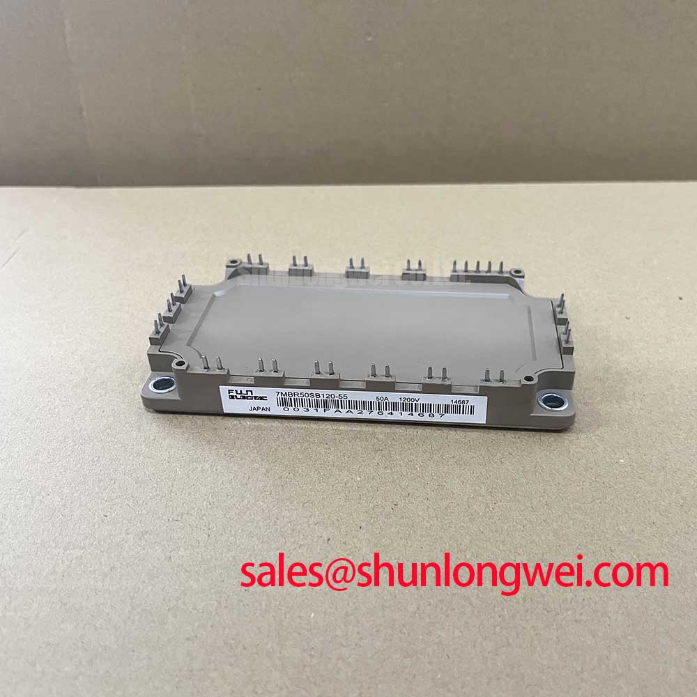
When a power conversion cabinet develops abnormal current imbalance or repeated inverter trips, isolate the DC link, verify that stored energy has been safely discharged, inspect the power module connections, and compare the installed device marking with the replacement specification before applying test power. The 7MBR50UH120 is a Fuji Electric PIM power module with a 1200 V voltage rating and a 50 A collector-current rating under the specified datasheet conditions.
Those figures define the principal product identification points for procurement and service work. They do not replace system-level checks covering switching frequency, load profile, gate-driver compatibility, thermal impedance, protection coordination, and DC-link transients. For commercial string inverters and micro-grid energy storage equipment, the replacement decision should be made against the original electrical topology and the installed cooling arrangement.
The module can be evaluated for inverter power stages where a high-voltage IGBT power module and its associated freewheeling paths are required. Before installation, record the original terminal arrangement, inspect the busbar contact surfaces, and confirm that the mechanical interface matches the existing heatsink and enclosure layout.
Peak junction temperature during a pulsed overload is governed by the complete thermal path rather than the current rating alone. The practical investigation starts with the load waveform, switching interval, conduction duty, case temperature, heatsink condition, and airflow through the cabinet. The 50.0 A rating is an official product parameter, while the permitted operating point in a particular inverter depends on the thermal network and the application conditions.
For a field assessment, capture the phase current and switching pattern during the event that produces the trip or thermal rise. A short overload can produce a different junction response from continuous full-load operation because the case temperature changes more slowly than the semiconductor junction. Engineers can represent this behavior with a multi-RC thermal model, using each thermal time constant to estimate the transient junction-temperature response to the power-loss pulse. The calculated peak junction temperature should then be checked against the applicable device and system limits during controlled testing.
Use the measured case temperature as the reference point for the thermal model. Check whether the heatsink is seated evenly, whether the thermal interface material has dried or migrated, and whether the airflow path is restricted by dust or cable routing. A calculated thermal margin is only meaningful when the assumed case temperature, power loss, pulse duration, and cooling conditions match the physical assembly.
Layout also affects the electrical stress that becomes thermal stress. Keep the commutation loop compact, route the gate-driver return separately from high-current paths where the topology permits, and reduce unnecessary stray inductance in the DC-link and phase-current connections. The system engineer should verify overshoot at the module terminals with suitable differential probing during switching tests, especially when a replacement module is installed in a busbar arrangement that differs from the original.
For service teams working on inverter cabinets, thermal imaging is useful after the system reaches a stable operating condition. Compare corresponding phase connections and look for localized heating at the terminal, busbar, or heatsink interface. A warmer area may originate from contact resistance, uneven clamping, airflow disturbance, or current imbalance, so the image should be interpreted alongside measured current and voltage waveforms rather than treated as a single-cause diagnosis.
Preventive maintenance should include heatsink cleaning, inspection of fan operation, and review of the thermal interface condition whenever the module is removed. ⚠️ Maintenance Note: monitor contact temperature during scheduled load checks and recheck the cooling path after any cabinet service.
Benchtop Waveform Tuning: Mitigating Bolted Contact Oxidation and Gate Noise on 7MBR50UH120
Bolted terminal joints deserve the same attention as the semiconductor itself because a small increase in contact resistance can create local heating under sustained inverter current. A micro-ohmmeter is appropriate for comparing the assembled joint with a known-good connection, provided the test leads are arranged for a four-wire measurement and the busbar is isolated from parallel current paths. The measured value should be interpreted against the assembly specification and the equipment manufacturer’s maintenance procedure rather than treated as a universal pass or fail threshold.
Inspect mating surfaces for oxidation, contamination, uneven pressure marks, and mechanical distortion. Clean and prepare the joint using a method compatible with the terminal finish. Reassemble the connection with controlled tightening practice and confirm that the busbar is not pulling the module terminal sideways. A thermographic scan under a stable load can then show whether the joint temperature profile is consistent across the phase connections.
The waveform review should cover both the IGBT switching edge and the antiparallel diode recovery interval. Excessive ringing at the switching node can result from the interaction of commutation inductance, device capacitances, diode reverse recovery, and probe placement. Compare the waveform at the module terminal with the gate-emitter waveform at the module pins. A clean driver waveform measured far from the power module does not prove that the gate-emitter voltage is equally well controlled at the device terminals.
| Evaluation item | 7MBR50UH120 | Service decision point |
|---|---|---|
| Manufacturer | Fuji Electric | Match the installed equipment documentation and module marking |
| Product category | PIM power module | Confirm the inverter topology and terminal arrangement |
| Rated voltage | 1200.0 V | Check DC-link transients and switching overshoot in the target system |
| Rated collector current | 50.0 A under the specified datasheet conditions | Compare continuous and pulsed load conditions with the cooling design |
| Related selection reference | 7MBP50RJ120 | Evaluate only after confirming topology, ratings, package, and control compatibility |
The related Fuji Electric reference above may be reviewed during a cross-check, but it should not be treated as an automatic substitute. The engineer responsible for the equipment must compare the electrical function, internal configuration, pin assignment, protection behavior, mechanical footprint, and thermal interface before approving any alternate part number.
Snubber selection is a system-level activity. An RC or RCD network can reduce ringing when its impedance and energy rating are suited to the measured commutation event, but an unsuitable network can increase switching loss or alter the intended waveform. Tune the network from oscilloscope evidence, then confirm semiconductor temperature, conducted noise, and radiated emissions under the actual operating load. A power module should not be described as independently carrying an entire inverter’s EMC compliance claim; compliance belongs to the assembled equipment and its verified test configuration.
Fuji Electric’s semiconductor resources at Fuji Electric Europe Semiconductor & Power Electronics provide useful manufacturer-level context for power semiconductor evaluation. Product integration still requires the correct documentation for the specific module and equipment revision.
Preventing Spurious Faults: Gate Driver Auxiliary Power Sequencing and Electrical Stress Guidelines for 7MBR50UH120
Gate-driver auxiliary power should become valid before the high-voltage DC link is applied. The practical sequence is to establish the driver supply, confirm the driver’s undervoltage lockout state, verify that the commanded turn-off condition is present, and only then permit the power stage to receive DC-link energy. The exact positive and negative gate-bias values must be selected from the driver design and the applicable module documentation; they should not be inferred from the module’s 1200.0 V rating.
An active negative turn-off bias can help resist unintended turn-on in a high dv/dt environment, but its value, source impedance, clamp behavior, and transient capability are determined by the gate-driver circuit. If the negative rail collapses during a fast switching event, the gate-emitter waveform may show displacement or ringing even though the driver supply appears correct during a static measurement. Probe directly at the module gate and emitter terminals, use a short measurement loop, and compare the result with the driver’s intended logic state.
Common-mode ground bounce should be addressed through layout rather than software timing alone. Keep the power-return path and control-return path organized according to the isolation architecture, minimize the area exposed to high-current commutation fields, and place desaturation, fault, and gate-clamp components close to the driver interface. The system designer should verify isolation clearances and creepage distances against the applicable equipment standard, pollution environment, and enclosure conditions.
Undervoltage lockout interlocks should block switching until the auxiliary supplies are stable. During troubleshooting, monitor the driver supply, gate-emitter voltage, fault output, and DC-link enable signal on the same time base. A fault that appears only during DC-link energization may involve sequencing, isolation capacitance, protection timing, or an unintended gate transient. Treat the event as a timing relationship to be measured, not as proof of an internal module failure.
Fast semiconductor fuses and short-circuit protection must be coordinated with the power module and the DC-link architecture. The fuse’s let-through energy, interruption capability, wiring inductance, and available fault current all affect the result. An I²t comparison can support the protection review, but the final coordination must include the actual fuse family, bus structure, fault path, and required disconnection time. A fuse cannot be assumed to prevent every semiconductor short-circuit consequence.
For cabinet installations exposed to condensation or seasonal humidity, inspect the driver board, isolation barriers, connectors, and module mounting area for contamination and moisture tracking. Allow equipment to reach a stable, dry condition before high-voltage testing. This is especially relevant when an inverter is moved between a conditioned service area and an outdoor energy-storage enclosure.
Transient Dynamics & Electrical Design: Antiparallel Freewheeling Diode Reverse Recovery on 7MBR50UH120
The antiparallel freewheeling diode influences turn-on stress, current overshoot, switching loss, and electromagnetic noise in the inverter leg. During bench testing, examine the diode current transition, the opposing IGBT collector-emitter voltage, and the gate-emitter waveform together. Reverse recovery behavior is shaped by junction temperature, forward-current history, commutation rate, stray inductance, and the gate-drive impedance selected by the system designer.
A snappy recovery event can produce a steep current change through the commutation loop. The resulting voltage excursion is related to the parasitic inductance and the rate of current change, so the correct response is to improve the physical loop and then tune the switching edge using measured data. Avoid adding damping components solely to suppress a ringing frequency observed with a long probe ground lead; first confirm that the waveform represents the module terminals.
Turn-on gate resistance can be adjusted as a typical bench-tuning starting point when the driver and module documentation permit adjustment. Increase damping only while checking switching loss, junction temperature, fault behavior, and the required dead time. A slower turn-on may reduce overshoot but can increase the voltage-current overlap during switching and thermal dissipation. The acceptable balance is determined by the inverter’s operating envelope rather than by a universal resistor value.
Use differential voltage probes and current probes with bandwidth appropriate to the switching event, and keep the measurement loop short. Compare repeated pulses at controlled temperature before changing the snubber or gate network. If the reverse-recovery current is asymmetric between phases, inspect the busbar geometry, diode current path, terminal contact, and driver timing as a combined system.
When the module is considered for a commercial string inverter or micro-grid storage converter, validate the complete power stage under the intended DC-link range, load profile, cooling condition, and protection sequence. The Power Electronics Masterclass offers broader guidance on IGBT selection and system reliability, while the product-level decision remains tied to the confirmed characteristics of the 7MBR50UH120 and the equipment’s verified electrical and mechanical interfaces.