Home » Library » APPLICATION OF IGBT DRIVE AND PROTECTION CIRCUIT
APPLICATION OF IGBT DRIVE AND PROTECTION CIRCUIT
Posted on: 10/26/2021
Insulated Gate Bipolar Transistor (IGBT), also known as insulated gate transistor. Because it has a parasitic thyristor inside the IGBT, it can also be called an insulated gate thyristor. It is a new type of composite device developed in the mid-1980s. Because it combines the advantages of MOSFET and GTR, it has the advantages of high input impedance, fast speed, good thermal stability and simple driving circuit, and has the advantages of low on-state voltage and high withstand voltage. , is popular with manufacturers and users. IGBTs have a tendency to replace MOSFETs and GTRs in motor drive, IF and switching power supplies, and in areas where fast, low loss is required. However, in the practical application of IGBT, one of the important issues to be considered is the protection problem of IGBT. Here, a simple and suitable protection circuit is designed and achieved very good results.
IGBT drive
1. IGBT gate drive voltage Uge
The driving conditions of the IGBT are closely related to the characteristics of the IGBT. When designing the gate driving circuit, the IGBT can be turned on when the gate driving voltage is greater than the threshold voltage. In general, the threshold voltage Uge(th)=5 to 6V. In this way, the IGBT can be fully saturated at the time of turn-on, the on-state loss is minimized, and the short-circuit current can be limited. Therefore, the gate drive voltage Uge needs to select a suitable value to ensure reliable operation of the IGBT. When the gate voltage is increased, it is beneficial to reduce the turn-on loss and conduction loss of the IGBT, but at the same time, the short-circuit time that the IGBT can withstand is shortened (below 10 μs), so that the freewheeling diode reverse recovery overvoltage increases, so it is necessary to Control the variation range of the gate voltage. Generally, the Uge can be selected between -10 and +15V, the turn-off voltage is -10V, and the turn-on voltage is +15V. Therefore, the gate driving voltage Uge ≥ D × Uge (th) is usually selected, and the coefficients D = 1.5, 2, 2.5, and 3. When the threshold voltage Uge(th) is 6V, the gate driving voltage Uge is 9V, 12V, 15V, 18V, and 12V is optimal. When the IGBT is turned off, the gate is negatively biased to improve the short-circuit resistance against load and the false trigger caused by du/dt.
2. IGBT gate resistance Rg
Choosing the appropriate gate series resistance Rg is important for IGBT drive. When Rg increases, it will increase the turn-on and turn-off time of the IGBT, and increase the power consumption of turn-on and turn-off, but at the same time, it can reduce the reverse recovery overvoltage of the freewheeling diode and reduce the influence of EMI. When the gate resistance is reduced, the di/dt is increased, which may cause the IGBT to be turned on. When the Rg is decreased, the IGBT switching time is reduced and the switching loss is reduced. However, if the Rg is too small, the oscillation between g and e may occur. The IGBT collector di/dt increases, causing the IGBT collector spike voltage to damage the IGBT. Therefore, Rg values should be selected according to IGBT current capacity and voltage rating and switching frequency, such as 10Ω, 15Ω, 27Ω, etc. It is recommended to connect Rge with a value of 10kΩ in parallel between g and e to prevent gate damage.
1. Design ideas
These drive integrated circuits have the potential to cause the IGBT to repeatedly withstand large current pulses of a few milliseconds while the load is continuously shorted. A strong current pulse during a short circuit threatens the safety of the IGBT and may cause irreversible damage. Therefore, in the event of a load short circuit, the working time of the IGBT short-circuit overcurrent must be reduced as much as possible. This requires the input circuit to be blocked by the external circuit to prevent the IGBT from continuously passing large current pulses. The driver integrated circuit alone is not sufficient to completely protect the IGBT, and an auxiliary protection circuit must be added to cut off the input drive signal.
2. Hardware protection circuit composition
This article can effectively achieve overcurrent and short circuit protection through LM358 and LS373. The circuit is mainly composed of an LM358, two diodes, an address latch LS373, two reference voltages and the like.
2.1 Characteristics of the LS373 chip
The LS373 is an eight-D transparent latch with a three-state output. The external pins and logic are shown in Figure 1.
Application Research of IGBT Drive and Protection Circuit
The output terminals 1Q to 8Q of the LS373 can be directly connected to the bus. When the three states allow the control terminal OE to be low, 1Q to 8Q are normal logic states and can be used to drive the load or the bus. When OE is high, 1Q~8Q is in a high-impedance state, neither driving the bus nor the load of the bus, but the logic operation inside the latch is not affected. When the latch enable terminal LE is high, Q varies with the data D. When LE is low, Q is latched at the established data level. When the input of the LE-terminal Schmitt trigger has hysteresis, the AC and DC noise immunity can be improved by 400mV. Terminal symbols: 1D ~ 8D for the data input, OE three-state allows the control terminal (active low), LE latch enable, 1Q ~ 8Q for the output. The truth table is shown in Table 1.
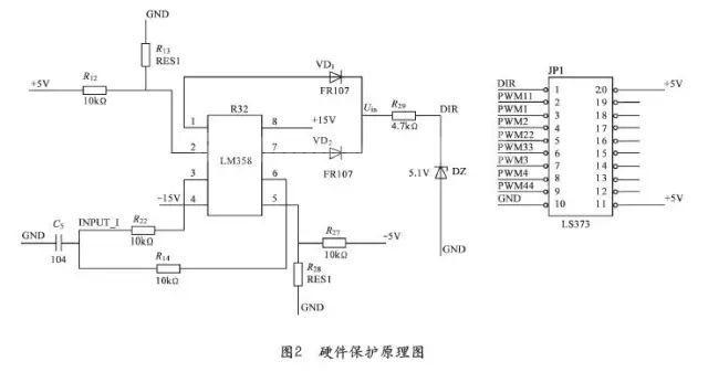
2.2 Hardware protection circuit analysis
Application Research of IGBT Drive and Protection Circuit
Also known as a double limit comparator. The reference voltage is +5V and -5V. When the input voltage UINPUT<-5V, the op amp LM358 outputs -15V. At this time, the diode VD1 is turned off, VD2 is turned on, Uin=12.96V, UDIR=5V, according to the truth table, LS373 The output is high impedance, the PWM output is blocked from the hardware, UDIR=0V, and the optocoupler is turned on (see Figure 3).
F is low; when the input voltage is -5V<UINPUT<+5V, the op amp LM358 outputs -15V, VD1 is cut off, VD2 is cut off, Uin=0V, UDIR=0V, because ENABLE of LS373 is high level, so The input signal is consistent with the output signal, UDIR=5V, the optocoupler is off, F is high; when the input voltage UINPUT>+5V, the op amp LM358 outputs +12.95V, VD1 is on, VD2 is off, Uin=12.96V, UDIR=5V. Similarly, the output of LS373 is high impedance and the PWM is blocked. UDIR=0V, the optocoupler is on, and F is low.
2.3 Software Protection Circuit Analysis
The overcurrent protection measures that are usually taken are hardware shutdown and software shutdown. Hardware shutdown means that when the overcurrent and short circuit signals are detected, the output of pin 1 of LS373 is high, which quickly blocks the gate signal and turns off the IGBT. However, since the hardware shutdown is turned off once the overcurrent signal is detected, the PWM11 to PWM66 outputs are constantly hopping, and it is easy to malfunction. In order to improve the anti-misoperation capability of the protection circuit, a software blockade is added after the hardware short circuit protection signal, that is, by the F signal (see Fig. 3). When UDIR
When it is high level, LS373 directly blocks the signals of PWM11~PWM66 to realize the hardware blocking signal. At the same time, UDRIVE becomes low level, the F signal is pulled low, and the PWM1~PWM6 signals are blocked by DSP software, thus playing the role of software protection. .
3. Protection process
When the voltage signal -5V<UINPUT<+5V, UDIR=0V, the F signal is high level, the hardware is not protected, the software is not protected; when the voltage signal UINPUT>+5V, UDIR=5V, hardware protection, blocking PWM At the same time, UDIRVE=0V, the optocoupler is turned on, F is low, and the DSP will block the PWM from the software. As the current decreases, the voltage signal UINPUT will be less than +5V and the hardware protection UDIR=0V, but at this point the software will block the PWM until it is powered back on. Similarly, when the voltage signal UINPUT<-5V, UDIR=5V, hardware protection, block PWM, at the same time, UDIRVE=0V, the optocoupler is on, F is low, the DSP will block the PWM from the software. As the current decreases, the voltage signal UINPUT will be less than +5V, and the hardware protection UDIR=0V. This overcurrent protection, once activated, will be restored by normal operation.
Experimental result
Application Research of IGBT Drive and Protection Circuit
Figure 6 shows that when the current signal makes the voltage +4.9V, that is, less than the reference voltage of 5V, there is no hardware protection, the F signal is also high level, and the voltage of the PWM output is about 15V, which is the driving voltage of the IGBT. Figure 7 shows that when the current signal makes the voltage 5.1V, that is, greater than the reference voltage 5V, UDIR=5V, hardware circuit protection, F signal is low level, blocking PWM, so that the PWM output voltage is 0V, that is, IGBT is not Drive voltage. Experiments show that when the actual voltage is less than -5V, the IGBT drive voltage is also 0V. Therefore, the LM358 and LS373 address registers can effectively protect the IGBT.
Conclusion
(1) The hardware protection is realized by blocking the PWM pulse by LS373, which can reliably protect the IGBT and prolong the service life of the IGBT.
(2) At the same time of hardware protection, the F signal is pulled low through the triode and the optocoupler to realize DSP software protection and improve the reliability of IGBT protection.