

Content last revised on September 17, 2026
Transient Dynamics & Electrical Design: Gate Trigger Current Considerations for AT671S45
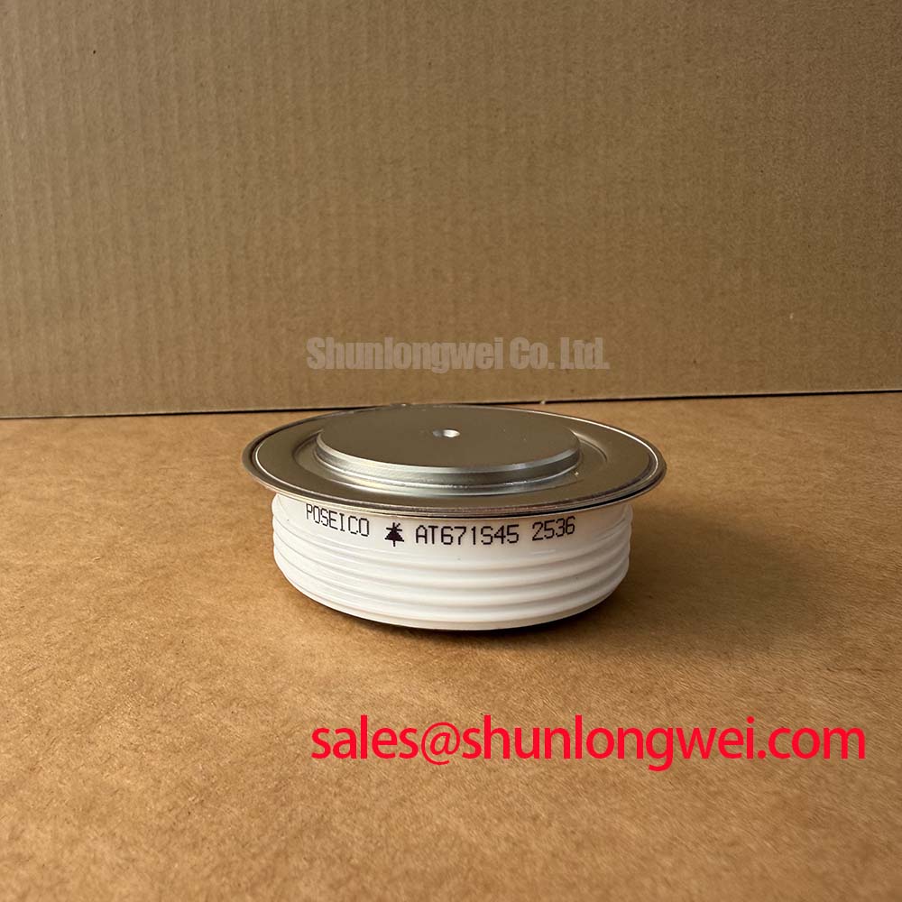
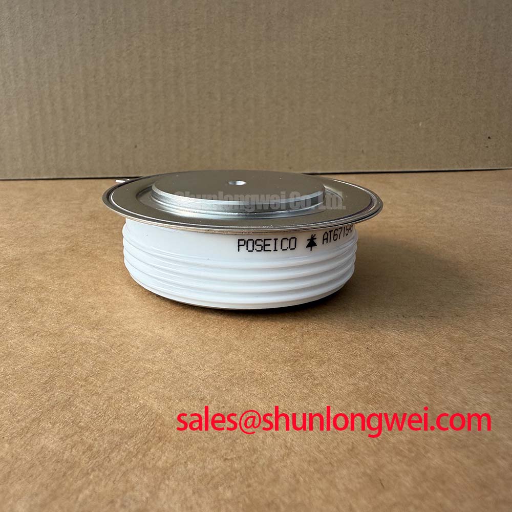
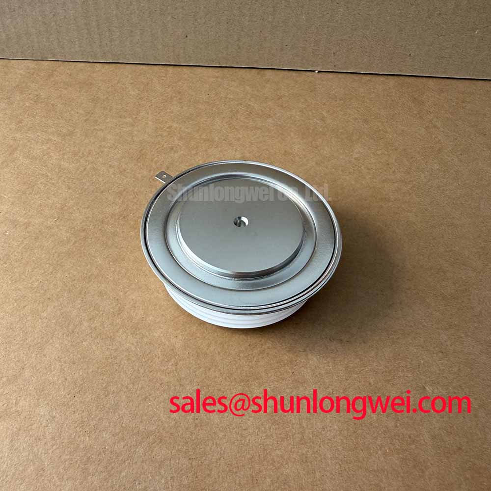
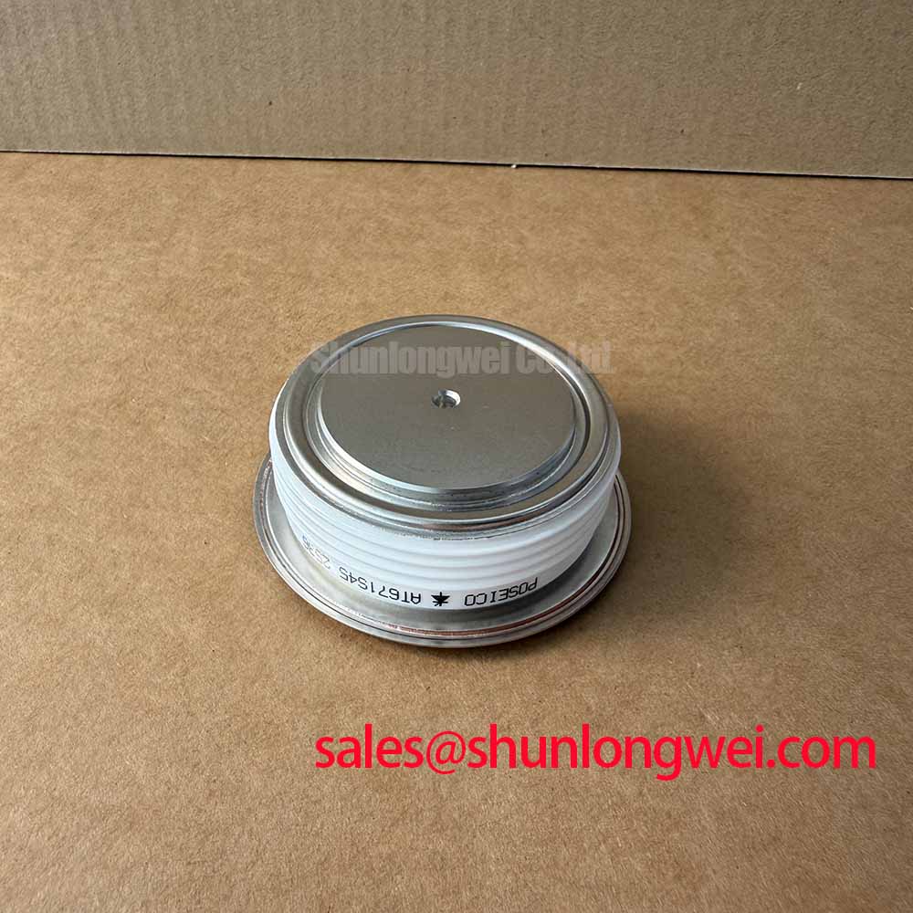
Before connecting a replacement device, isolate the rectifier, confirm the terminal identification against the original assembly documentation, and inspect the clamping faces, conductors, and gate connections for looseness or heat discoloration. The AT671S45 is a Poseico thyristor module with an official repetitive peak reverse voltage rating of VRRM = 4500 V, a mean on state current rating of IT(AV) = 1085 A at Th = 55 C, and a surge on state current capability of ITSM = 13.0 kA for 10 ms. These are Official Datasheet Specifications and define the electrical boundary that must be checked against the installed rectifier design.
The supplied official parameter set does not state gate trigger current, gate pulse rise time, holding current, latching current, gate reverse voltage, or gate power limits. These values should be verified from the original Poseico documentation and the existing firing board records before an AT671S45 is energized. A gate transformer or pulse driver that was acceptable for another thyristor family cannot be assumed to provide the correct trigger behavior for this device.
Design Consideration: in high current phase controlled rectifiers, a clean firing pulse must arrive at the gate with adequate rise characteristics and sufficient duration for the actual load current to establish conduction. The system engineer should inspect the gate and cathode return path as a pair, because shared current paths can introduce common mode disturbance during commutation. Where the original hardware uses separate gate return conductors, preserve that routing rather than combining it with a high current terminal path.
For multi pulse firing systems, verify firing symmetry across the bridge before attributing uneven load current to the thyristor itself. Oscilloscope measurements should be referenced to the approved test method for the firing circuit, with suitable isolation and voltage safety controls. A weak, delayed, or distorted pulse may indicate a driver, connector, transformer, or return path issue; it does not establish a single device fault by itself.
| Official Specification | Value | Integration Relevance |
|---|---|---|
| Repetitive peak reverse voltage, VRRM | 4500 V | Reverse blocking boundary for the installed rectifier topology |
| Mean on state current, IT(AV) | 1085 A at Th = 55 C | Continuous current reference under the specified cooling condition |
| Surge on state current, ITSM | 13.0 kA for 10 ms | Fault and inrush coordination reference |
| I2t value | 845 kA2s | Reference for semiconductor fuse coordination |
| On state slope resistance, rT | 0.700 mOhm | Conduction loss assessment input |
| Threshold voltage, VT(TO) | 1.20 V | Forward characteristic assessment input |
Assembly Integrity & Layout Architecture: Implementing Critical Rate of Rise of Off State Voltage for AT671S45
Inspect the busbar stack, snubber leads, gate leads, and heatsink interface before commissioning. The official specifications supplied for the AT671S45 do not include a critical rate of rise of off state voltage rating. Therefore, no device specific dv/dt limit should be inferred from the 4500 V reverse voltage rating. The system integrator should obtain the applicable dv/dt limit from original manufacturer documentation and evaluate it using switching waveforms measured in the installed equipment.
Design Consideration: RC snubber networks and series reactors are commonly evaluated to moderate voltage transition stress and current rise in phase controlled power stages. Their required values depend on the transformer leakage inductance, busbar geometry, line impedance, commutation conditions, and the measured waveform at the device terminals. Component selection must be validated by the system engineer while verifying peak voltage margins against the installed DC or line voltage during switching tests.
Keep snubber connections physically short and connected to the intended power terminals, because added loop area can reduce the effectiveness of a network intended to control transient behavior. Ferrite components can also be considered in control wiring where high frequency interference is observed, subject to measurement of the affected signal path. The operating principles of a ferrite core and a ferrite bead are relevant to suppressing high frequency disturbances, but neither substitutes for correct power loop layout.
Field Alert: De-energize, discharge, and verify the power assembly is safe before removing gate, snubber, or busbar connections.
Mounting torque, thermal compound thickness, creepage distance, and clearance must follow the original module drawing, heatsink design, terminal hardware specification, and applicable equipment safety requirements. The supplied factory data does not state mounting torque or package dimensions. Do not transfer torque settings from a superficially similar module. Uneven clamping can affect thermal contact and terminal reliability, particularly where the rectifier has sustained high current duty.
When reviewing related rectifier positions, the TT500N18KOF can be examined as a separate device reference for topology documentation and original bill of materials comparison. Its ratings, terminal arrangement, triggering requirements, and mechanical drawing must be evaluated independently.
Assembly Integrity & Layout Architecture: Evaluating Post-Surge Reverse Voltage Blocking for AT671S45
After a suspected line fault or inrush event, begin with a powered down inspection of the fuse indicators, busbar joints, cooling path, gate wiring, and visible insulator condition. The AT671S45 official surge rating is ITSM = 13.0 kA for 10 ms. This identifies a specified short duration surge capability, not a permission to repeat fault tests or a prediction of remaining service life after a fault event.
The official I2t = 845 kA2s value is an important coordination input when the rectifier uses high speed semiconductor fuses. Fuse selection cannot be finalized from I2t alone. The protection engineer should assess the prospective fault current, clearing characteristic, coordination with upstream protection, cable impedance, and the complete time current behavior of the installed circuit. Replace operated protective parts according to the equipment service procedure before applying voltage again.
Design Consideration: reverse blocking should be assessed only after the thermal condition, circuit integrity, and measured device waveforms are understood. A post surge insulation check that appears abnormal may involve the device, a contaminated interface, a damaged snubber, a conducting parallel path, or the test arrangement. Compare readings with an approved known good phase or documented service limits, while observing the instrument manufacturer safety method.
A high current green hydrogen electrolyzer DC power rectifier is one potential application where engineers may evaluate this voltage and current class, subject to the original topology, thermal system, and firing architecture. The 1085 A mean current rating is stated at Th = 55 C with double sided cooling. It must not be treated as an unconditional cabinet level current rating where cooling conditions differ.
For a documented cross model assessment, SSIL2890S46C should be compared only through its own official electrical, thermal, mechanical, and gate specifications. Pin connections, voltage class, current conditions, cooling arrangement, and protection coordination require direct verification before any replacement decision.
AT671S45 Operational Boundaries: Evaluating Surge Energy Dissipation and Clamping-Voltage Limits
Start surge protection troubleshooting at the incoming AC protection stage and trace the path toward the thyristor bridge. Check whether MOV assemblies, RC snubbers, surge arresters, fuses, contactors, and their interconnections match the original equipment documentation. The AT671S45 has an Official Datasheet Specification of VRRM = 4500 V, but the supplied data does not provide a device specific surge energy rating, clamp voltage rating, avalanche rating, or an IEC 61000 4 5 compliance claim.
Design Consideration: MOV and RC snubber stages may be evaluated as system level protection elements when line disturbances or switching transients can impose excess stress on a thyristor rectifier. Their energy handling, clamping behavior, placement, coordination with fuses, and degradation monitoring are determined by the measured surge environment and the protected equipment design. The system engineer should verify transient voltage at the AT671S45 terminals under representative conditions rather than relying on nominal supply voltage alone.
The official forward characteristic inputs, VT(TO) = 1.20 V and rT = 0.700 mOhm, support conduction loss calculations within the conditions defined by the original data. They do not establish a complete thermal result without the installed current waveform, duty cycle, cooling arrangement, interface condition, and thermal path. Review these conditions when a rectifier phase shows a recurring temperature imbalance.
For display and control station documentation associated with long service equipment, The Ultimate Guide to Industrial TFT LCD Technology provides a separate reference for industrial display integration. It does not define the electrical limits, surge capability, or firing requirements of the AT671S45.