Content last revised on September 13, 2026
Preventing Spurious Faults: Dynamic Gate Impedance Control Guidelines for CM1200HA-34H
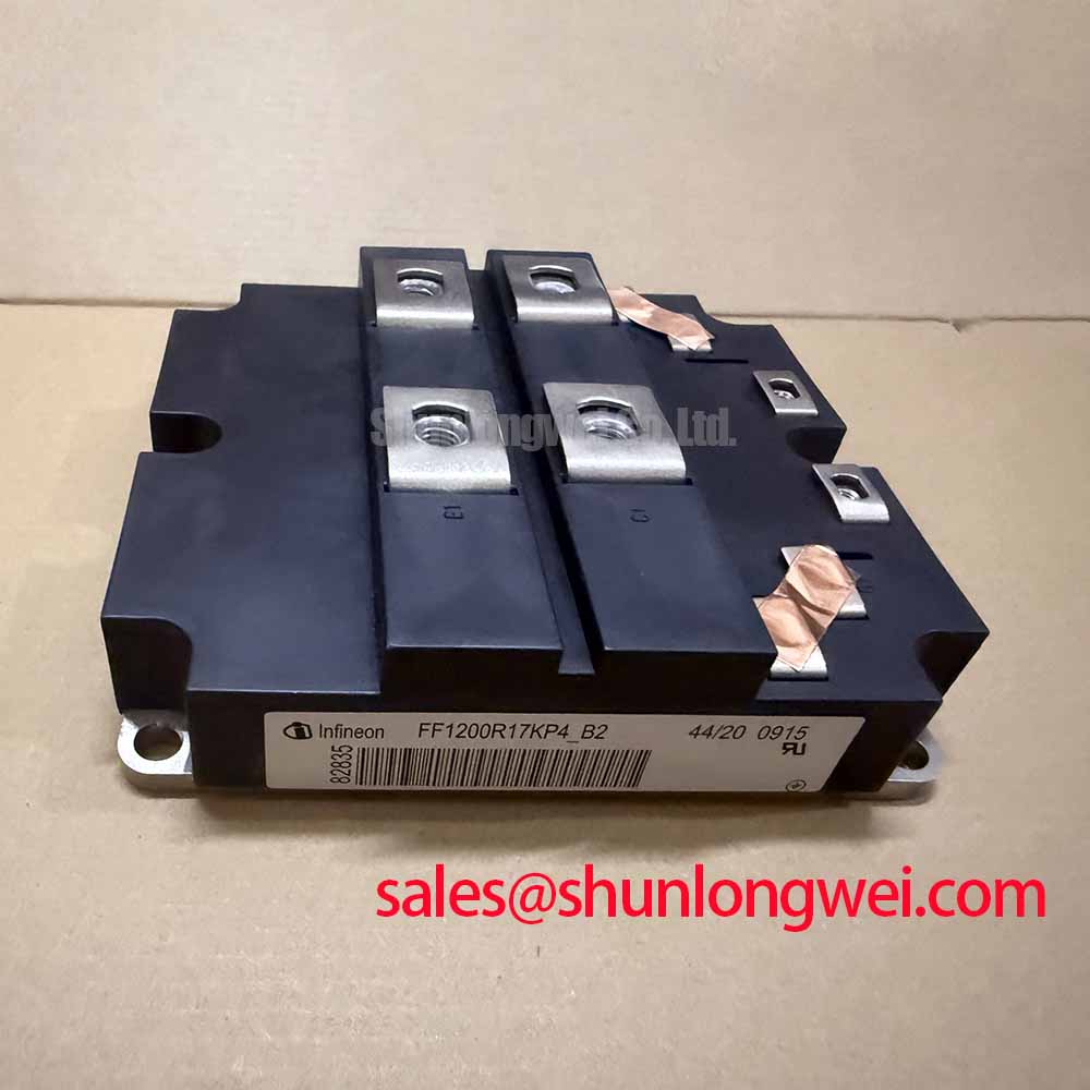
Before energizing any test fixture, verify the marking for CM1200HA-34H, inspect the module case and terminals, and record a cold-state reference for the power and gate terminals with the device isolated from every external circuit. Mitsubishi Electric identifies this device as an IGBT Module with an official rated voltage of 1700.0 V, an official rated current of 1200.0 A, and a Module package. These are product-level specifications; switching frequency, gate voltage, short-circuit withstand, thermal impedance, isolation rating, and surge capability must be confirmed from the applicable manufacturer documentation before a replacement is commissioned.
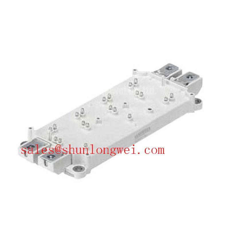
For incoming inspection, compare the terminal arrangement with the original equipment drawing rather than assuming that a visually similar high-power module has the same internal topology. Confirm polarity and terminal identity using the machine schematic, then use a current-limited meter procedure appropriate for a disconnected power semiconductor. A diode-test reading across a freewheeling path can provide a cold-state comparison, but it does not prove dynamic switching performance or semiconductor integrity. Gate-to-emitter checks should be performed with suitable electrostatic discharge controls and without applying uncontrolled external voltage.
| Item | CM1200HA-34H information | Engineering classification |
|---|---|---|
| Manufacturer | Mitsubishi Electric | Official product identification |
| Device category | IGBT Module | Official product classification |
| Rated voltage | 1700.0 V | Official specification supplied for this product page |
| Rated current | 1200.0 A | Official specification supplied for this product page |
| Package | Module | Official package description supplied for this product page |
When this module is evaluated in a high-power inverter leg, the gate-drive circuit should be treated as part of the switching power loop. A fast collector-emitter voltage transition can couple through the device capacitances and the common gate return, creating an unintended gate disturbance on the complementary switch. The result may appear as intermittent overcurrent, gate-driver shutdown, or a waveform that changes when the bus voltage or load current changes. These symptoms require oscilloscope comparison at the gate-emitter terminals and at the power terminals; they should not be assigned to the IGBT alone without checking the driver, return path, and probe arrangement.
A Design Consideration for this topology is to provide a controlled gate impedance path and a dedicated active Miller clamp where the driver architecture supports it. A negative turn-off bias may also be evaluated by the system designer when high dv/dt creates unwanted gate movement, but the actual bias must be selected from the complete gate-driver specification, insulation strategy, driver absolute maximum ratings, and the module manufacturer’s application data. The negative bias values sometimes used in high-power converters are not official CM1200HA-34H specifications and should not be copied into a production design without validation.
Keep the turn-on and turn-off gate paths physically defined, with the power commutation loop separated from sensitive control traces. Minimize parasitic loop inductance to reduce turn-off overshoot, and verify the resulting peak gate and collector-emitter voltages during switching tests. The control board should also be checked for common-mode transient immunity. Optical or digital isolation devices in the industrial drive board need a CMTI capability appropriate to the measured switching environment, while their supply bypassing and reference connections must remain consistent with the isolation design.
For a utility-scale 1500V high-power central solar photovoltaic inverter, compatibility assessment should include the actual DC-link operating range, modulation strategy, current waveform, fault response, and cooling assembly. The 1700.0V rating is an official device parameter, but it is not a substitute for system-level transient measurement. Designers should verify the peak voltage margin against switching overshoot, wiring inductance, regenerative events, and control timing. Mitsubishi Electric’s Power Semiconductors and High-Power Modules information should be consulted alongside the exact device documentation.
💡 Bench Tip: Use ESD protection and compare every cold-state measurement with a known-good reference module or the original equipment record before applying any gate-drive signal.
Field Diagnostics & Commissioning: Derating Guidelines and Mismatched Parameters in CM1200HA-34H Topologies
Commissioning should begin with the electrical topology, not with a presumed replacement relationship. Confirm whether the original circuit uses a single switching position, a paralleled arrangement, a chopper branch, or a regenerative braking path. In a large photovoltaic inverter, the module may be evaluated within a DC conversion or inverter stage, but the suitability of that position depends on the complete schematic and thermal design. The official 1700.0 V voltage and 1200.0 A current figures should be compared with the equipment documentation under its specified test conditions; they should not be interpreted as a universal operating point for every waveform.
For paralleled devices, the positive temperature coefficient commonly associated with IGBT saturation voltage can support static current sharing under suitable conditions. This is a Design Consideration, not a guaranteed sharing result for this specific module. Dynamic balance is more sensitive to gate-loop symmetry, emitter or return-path impedance, driver propagation mismatch, busbar geometry, and thermal coupling. Use matched physical routing where the equipment design calls for parallel operation, then verify current distribution with appropriate isolated measurement equipment during controlled load testing.
Mismatched gate resistors, unequal copper paths, or different driver supply behavior can produce unequal switching losses even when the static voltage drop appears similar. A field diagnostic review should therefore compare turn-on delay, turn-off delay, gate plateau behavior, collector-emitter overshoot, and temperature rise between corresponding positions. A difference that appears only during high current may involve commutation layout or measurement bandwidth rather than a simple static defect.
Fast semiconductor fuses should be assessed through the manufacturer’s published I²t clearing characteristics and the module’s documented surge and short-circuit limits. The fuse coordination must account for prospective fault current, DC-link energy, wiring impedance, and protection detection delay. No specific fuse size or I²t value can be assigned from the three supplied product parameters alone. During commissioning, record the actual protection sequence and confirm that the fuse, gate shutdown, contactor logic, and DC-link discharge strategy do not conflict with one another.
A neutral comparison may include FF45017ME4, but its electrical ratings, internal topology, terminal layout, and switching behavior must be reviewed independently. It should not be treated as an automatic substitute for CM1200HA-34H. In a wider power-conversion assembly, the CM100DY-12E may be relevant as a separately assessed front-end rectification or auxiliary-stage device, subject to the original topology and control requirements.
Assembly Integrity & Layout Architecture: Implementing Desaturation Detection for CM1200HA-34H
Desaturation protection is a system protection function that detects an abnormal rise in the conducting switch voltage while the gate command remains active. For CM1200HA-34H integration, the sensing network, blanking behavior, gate-driver supply, and fault latch should be checked against the actual switching waveform. A protection threshold that is suitable for one module family or gate driver is not automatically correct for another. The designer should validate the threshold with a controlled load and confirm that normal turn-on recovery, diode commutation, and measurement delays do not create nuisance trips.
Type-I and Type-II short-circuit behavior should be evaluated using the precise short-circuit safe operating area and time limits published for the device. The requested sub-cycle response must be treated as a system target, not as an official CM1200HA-34H parameter supplied here. The protection chain should detect the event, block the gate command, and communicate the fault to the supervisory controller quickly enough to remain within the documented device limits. Verification requires a high-bandwidth voltage measurement, a suitable current probe, and a known protection delay under the intended driver supply conditions.
Two-stage soft turn-off can be considered where an immediate gate discharge would create excessive inductive voltage. The first action reduces channel current under controlled gate impedance; the second completes the shutdown after the power-loop response has been observed. The timing and gate levels must be determined by the system engineer from measured overshoot, short-circuit current, driver capability, and the applicable manufacturer data. Minimize stray inductance in the gate and commutation loops, maintain adequate physical clearance for the working voltage, and keep desaturation traces away from high-current switching nodes.
During a fault investigation, inspect the desaturation diode path, blanking capacitor, isolated driver supply, fault latch, and control-board common-mode behavior as separate sections. An unexpected trip may indicate sensing layout sensitivity, driver supply disturbance, or an actual power-stage event. Compare the fault waveform with a known-good operating trace and confirm probe reference integrity before replacing the module. Mitsubishi Electric’s Global Semiconductor Device Technologies resource provides manufacturer-level context for power semiconductor evaluation.
Junction-to-Case Thermal Network Simulation Guidelines for CM1200HA-34H
Thermal evaluation should begin with the module’s documented junction-to-case transient thermal impedance curves and the actual case temperature measured at the specified reference location. A pulsed overload cannot be assessed reliably from steady-state resistance alone. In simulation, represent the transient thermal path with the manufacturer’s approved multi-RC network when available, then apply the real conduction and switching loss waveform rather than a constant average value. The calculated junction temperature should be checked against the applicable maximum rating and the complete operating profile.
The power loss model should include conduction loss, switching loss, reverse-recovery interaction where applicable, gate-drive loss, and the effect of current and temperature on the device characteristics. For a regenerative braking chopper, the model also needs the braking resistor duty cycle, DC-link energy, switching pattern, and cooling response. The resistor absorbs energy at the system level, while the IGBT still experiences thermal pulses during each conduction and switching interval. Designers should verify that the braking event does not create a transient junction temperature excursion that is hidden by a slower heatsink temperature measurement.
When a multi-RC model is unavailable, a Design Consideration is to use a conservative transient thermal representation and calibrate it against measured case temperature, switching loss, and load pulse duration. This is an Engineering Calculation, not an official CM1200HA-34H thermal specification. The result should be treated as a design estimate until it agrees with controlled laboratory measurements. Thermal interface condition, mounting flatness, clamping uniformity, airflow, coolant behavior, and neighboring module heating can all alter the case-to-heatsink path.
For field service, record the pre-event load profile, heatsink temperature, cooling status, gate waveform, and fault timestamp before dismantling the assembly. Inspect the mounting surface and interface material for uneven contact, but do not infer a precise interface thickness or mounting torque for this model without the applicable mechanical drawing. The Field Engineer’s Handbook can be used as a practical reference for structured testing, failure analysis, and reliability review. Any final approval for a 1500V central solar photovoltaic inverter should be based on the original application documentation, measured switching margins, verified protection coordination, and the manufacturer’s complete CM1200HA-34H data.