Content last revised on October 9, 2026
Field Diagnostics & Commissioning: Thermal Feedback in SEMIX604GB12T4S Topologies
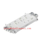
| Model | SEMIX604GB12T4S |
|---|---|
| Manufacturer | Semikron |
| Product category | IGBT Module |
| Package | SEMiX Module |
| Specified voltage rating | 1200 V |
| Specified current rating | 600 A |
Measure the disconnected module’s collector-to-emitter diode response in both polarities, using the terminal diagram to identify each measurement path. Disconnect external busbars and gate wiring where necessary to prevent surrounding circuitry from masking the result. Record meter polarity, module temperature, and readings against a known-good unit under the same conditions. A diode-mode reading is a screening observation, not a measurement of operating VCE(sat), blocking capability, or usable load current.
💡 Bench Tip: Keep the gate protected against electrostatic discharge and compare cold-state readings only after confirming that the DC link is discharged.
The 1200 V voltage rating and 600 A current rating describe different electrical boundaries; they must not be interpreted as simultaneous continuous operating capability. Current assessment requires the applicable pulse duration, case temperature, cooling conditions, and safe operating area. For procurement, retain the complete SEMIX604GB12T4S designation rather than matching only the voltage and current fields.
Design Consideration: When evaluating parallel branches, compare conduction voltage at matched current and temperature. A positive VCE(sat) temperature coefficient can assist steady-state sharing only in the operating region where the device characteristics establish that behavior. It does not guarantee equal switching current. Compare gate-loop routing, driver impedance, power connections, and thermal contact before attributing an uneven temperature rise to the semiconductor.
Replacement assessment also requires terminal geometry, gate-drive compatibility, and thermal-interface compatibility. The SKM100GB063D is a separate catalog reference for comparison, not an established interchangeable replacement. A matching product category alone cannot establish electrical or mechanical suitability.
Field Diagnostics & Commissioning: Common-Mode Transient Immunity in SEMIX604GB12T4S Topologies
Capture the gate-to-emitter waveform during switching transitions with a suitably rated differential measurement arrangement, then correlate unwanted gate pulses with driver input and supply behavior. Measure at the module-side gate reference rather than a distant control-board ground. Probe common-mode limitations and grounding errors can produce misleading traces, so validate the measurement setup before diagnosing a false turn-on event.
Design Consideration: Common-mode transient immunity belongs to the gate-driver isolation system, not to the IGBT module’s collector-to-emitter voltage rating. Evaluate the isolator, isolated power supply, PCB spacing, and return paths against the measured switching environment. Neither reinforced isolation nor a particular withstand voltage can be inferred from the SEMiX Module package designation.
For insulation assessment, distinguish the module’s power-terminal-to-baseplate requirements from the driver’s isolation-barrier requirements. Use the applicable manufacturer test conditions and equipment safety requirements to establish the test voltage, duration, and leakage acceptance criteria. Disconnect circuitry that is not intended to participate in the test. An arbitrary high-voltage bench test can stress connected components without establishing useful system-level insulation evidence.
The Semikron-Danfoss official power electronics hub provides manufacturer resources for device-specific documentation. Its MiniSKiiP power-module information concerns a different product family; its mounting and connection arrangements should not be transferred to this SEMiX module.
When evaluating a high-speed rail or heavy freight locomotive traction inverter, engineers should establish compatibility with its existing driver, cooling assembly, insulation coordination, and qualification requirements. This is an application assessment, not a claim that the module carries railway approval or is a direct replacement for a particular traction assembly.
Benchtop Waveform Tuning: Negative Gate Bias and Active Miller Clamping on SEMIX604GB12T4S
Inspect the off-state gate waveform while the opposing switch changes state, looking for gate excursions that coincide with collector-voltage transitions. Compare the trace with driver supply behavior and the local emitter reference. An excursion may reflect Miller coupling, shared return-path inductance, probe pickup, or driver behavior; the waveform alone does not identify a single cause.
Design Consideration: Negative gate bias and active Miller clamping are driver-level methods for controlling unintended turn-on. Their suitability depends on the module’s permitted gate-voltage range, the driver’s clamp implementation, and measured transients. Determine the actual bias and clamp arrangement from those constraints rather than assigning a generic negative voltage to SEMIX604GB12T4S.
Trace the gate return separately from high-current paths wherever the documented terminal arrangement permits. Do not assume the presence of a dedicated auxiliary emitter terminal from the model name. Compare wiring length and routing between parallel branches, then verify dynamic balance under representative switching conditions. Equal cold-state readings do not demonstrate equal turn-on or turn-off behavior.
Evaluate desaturation detection and soft shutdown together using an appropriately controlled test setup. Detection blanking must accommodate normal switching behavior without obscuring a fault, while shutdown must limit electrical stress within the documented short-circuit capability. A desaturation threshold is not simply the normal VCE(sat) value. Inspect driver undervoltage behavior and isolated supply stability as part of the same test, since supply disturbances can alter gate control and protection timing.
Assembly Integrity & Layout Architecture: Commutation Loop Inductance in SEMIX604GB12T4S
Measure collector-to-emitter turn-off overshoot at the module terminals and inspect busbar joints, capacitor connections, and the physical commutation path when the peak changes between assemblies. Compare equivalent load and temperature conditions. A distant DC-link measurement can miss local stress, while excessive probe-loop area can exaggerate it.
Engineering Calculation: The simplified relationship Vpeak = VDC + Lσ × di/dt explains why commutation-loop inductance adds voltage during a current transition. It is an estimate, not a complete switching model. Minimize the loop area and verify measured peaks against the module’s voltage boundary, allowing the system engineer to determine the required operating margin and suppression network.
Design Consideration: Select snubber components from measured ringing, pulse energy, component ratings, and thermal behavior rather than from a universal capacitance or inductance target. Review rectifier and DC-link behavior separately: front-end disturbances can affect the inverter supply but do not establish an IGBT fault. The SKM75GB07E3 is another IGBT-module reference for subsystem comparison, not an assumed rectifier or specified companion to this device.
Inspect mounting surfaces, interface condition, and fastener engagement using the module-specific assembly instructions. Do not import press-pack spring-loading procedures or assume double-sided cooling from unrelated package technologies. The article The Advanced Thermal Management Revolution offers broader cooling context, not mounting acceptance criteria. After correcting an assembly issue, repeat the same electrical and thermal measurements to determine whether the intervention changed the observed stress.