

Content last revised on October 2, 2026
Preventing Spurious Faults: Thermal Interface Material Thickness Guidelines for SKM800GA176D
Begin the thermal installation by cleaning the module baseplate and heatsink contact surface with a process approved for the equipment. Check the heatsink for burrs, embedded particles, local high spots, and visible curvature. A contaminated or uneven interface can create local thermal resistance and mechanical stress, even when the mounting screws appear tight.
Thermal interface material thickness is a process variable rather than an official SKM800GA176D electrical rating. An engineering recommendation may use a controlled thin layer, with a process window such as 50–100 μm only when supported by the selected material, surface flatness, and supplier instructions. The production team should validate the actual layer after compression instead of treating a nominal coating thickness as guaranteed across the complete baseplate.
Apply the material uniformly across the intended contact area and avoid trapped air pockets. Voids near the highest heat-flow region can produce a misleadingly acceptable cold inspection while causing uneven thermal behavior during load operation. If a module is removed and reinstalled, inspect the compressed interface rather than automatically reusing the previous material.
Use the manufacturer’s specified fastener sequence and torque data when available. If those details are not available for the exact Semitrans assembly, the mounting procedure must be established by the equipment designer and validated mechanically. A staged, diagonal tightening sequence is a general design consideration because it helps distribute pressure progressively; it is not an official SKM800GA176D mounting specification.
During troubleshooting, compare thermal images or temperature-sensor readings between equivalent phases only after confirming similar load current, airflow, switching conditions, and sensor placement. A hot region may be related to interface contact, current imbalance, gate timing, busbar resistance, or cooling performance. Verify each condition rather than assigning the temperature rise to the thermal compound alone.
💡 Bench Tip: Keep the module and test instruments within an ESD-controlled work area, then record cold-state resistance and diode-test observations before connecting the gate-drive harness or DC bus.
Preventing Spurious Faults: Suppression of DC-Link Voltage Doubling at Motor Terminals
Long motor cables can behave as transmission-line structures rather than simple conductors. Their impedance, termination, cable length, motor input characteristics, and switching edge rate can produce reflected voltage at the inverter output. Under unfavorable conditions, the terminal transient may approach a multiple of the DC-link voltage, placing additional stress on the IGBT module, motor insulation, and output switching network.
This behavior should be verified with a properly rated differential probe and a measurement layout that does not add excessive loop inductance. Compare the measured collector-emitter voltage and motor-terminal waveform at the inverter, cable termination, and motor side when practical. A spike visible at one location but absent at another may indicate reflection, probing influence, or a grounding problem rather than a direct semiconductor failure.
Output dv/dt filters, motor chokes, and common-mode components should be selected from the complete drive topology. The required attenuation depends on DC-link voltage, motor cable characteristics, switching pattern, motor insulation limits, thermal loss, and allowable output waveform distortion. Designers should verify the resulting peak voltage during switching tests instead of applying a universal filter value to every traction inverter.
Overvoltage protection may include a coordinated network using a metal-oxide varistor, clamp elements, snubbers, or an active braking path. An MOV should not be selected only from its nominal voltage label. Its continuous operating voltage, transient energy, clamping behavior, leakage, coordination with the DC-link protection, and thermal clearance require review. The protection network also needs a defined fault-current path so that a failed suppressor does not create a new short circuit across the bus.
Gate-drive sourcing and sinking capability must be evaluated together with the actual gate charge, driver supply, isolation device, gate-loop inductance, and required switching speed. External gate resistance is a tuning element, not a fixed attribute of the module. Increasing resistance can reduce ringing and edge speed while increasing switching loss; reducing it can improve switching speed while increasing overshoot and electromagnetic disturbance. Select the value through measured gate-emitter and collector-emitter waveforms, with the final limits determined by the drive system.
For isolated gate-drive boards, review the common-mode transient immunity of the optocoupler or digital isolator, the isolation barrier layout, and the return-current path. The component itself does not independently certify the complete traction inverter for CISPR or other EMC requirements. The finished equipment must be evaluated under its intended cable, enclosure, grounding, and switching conditions. The Semikron-Danfoss SEMITRANS® Industry Standard IGBTs resource provides useful manufacturer-level context for the product family, while the Semikron-Danfoss Power Electronics and Modules hub should be consulted for current technical documentation.
Field Diagnostics and Commissioning: Static and Dynamic Current Distribution in SKM800GA176D Topologies
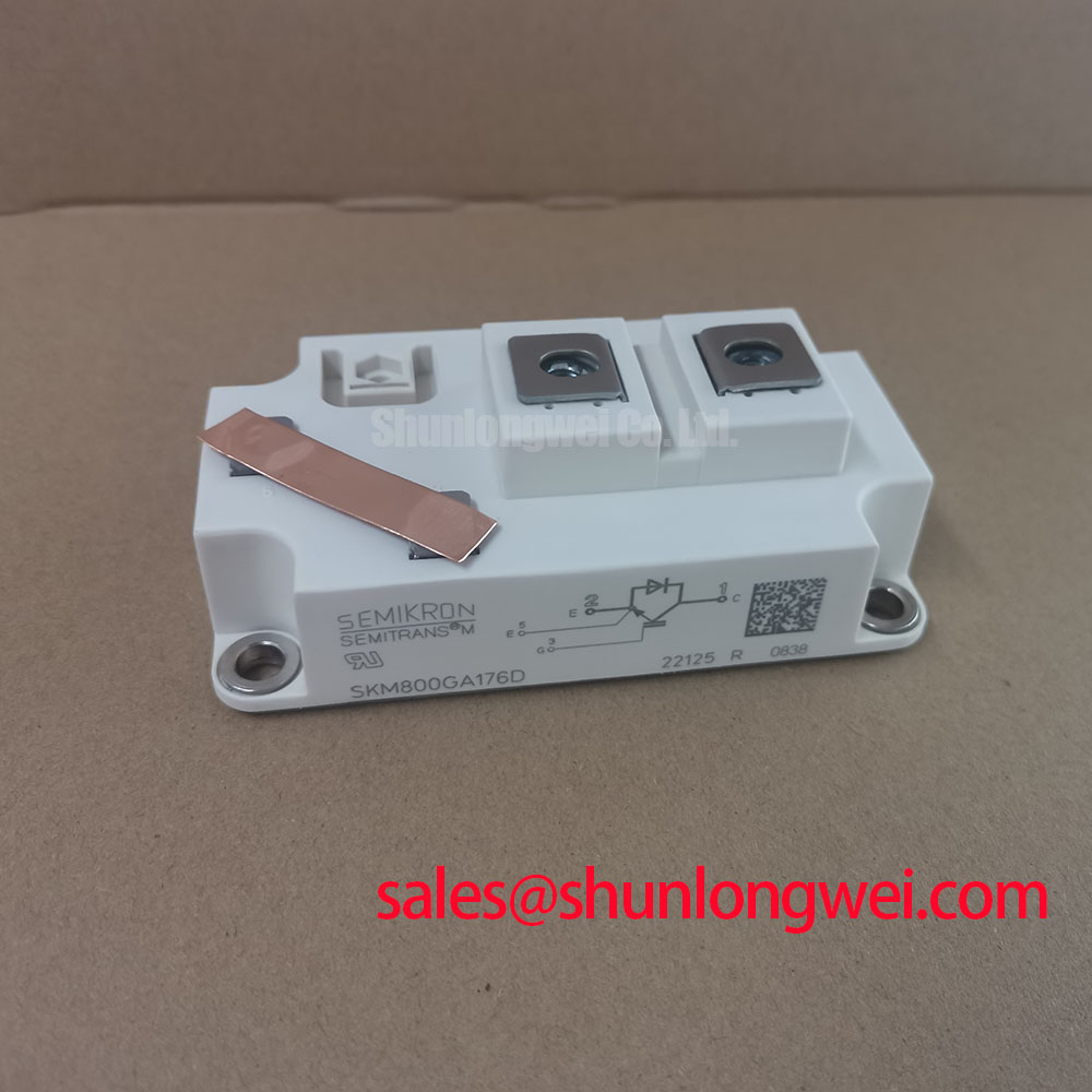
Incoming inspection should begin with the module disconnected from every powered circuit. Identify the power terminals and gate-drive terminals from the exact drawing for the part and equipment revision; do not infer pin functions from another Semitrans device. In diode-test mode, record the polarity and forward-voltage indication of each accessible antiparallel diode path, then compare the readings with a known-good module under the same instrument range and lead arrangement.
A diode-test result is a screening observation, not a complete semiconductor health certificate. Unexpected conduction in both directions, a persistent open reading where a diode path is expected, or a strong difference between matched devices should lead to further isolation testing. Check whether a snubber, gate resistor, current sensor, or parallel board path is influencing the reading before attributing the result to the IGBT die.
For parallel current paths, the positive temperature coefficient commonly associated with IGBT conduction voltage can support static current sharing, but the complete result depends on device matching, thermal coupling, busbar resistance, emitter connections, and operating point. This is a design consideration, not a guaranteed current-sharing value for the SKM800GA176D without the relevant manufacturer curves and application conditions.
Dynamic sharing is more sensitive to wiring symmetry. Keep the gate-drive paths physically equivalent, avoid routing one gate loop beside a high-current commutation path, and verify the return connection specified by the original circuit. The supplied product information does not confirm a Kelvin emitter auxiliary terminal for this model, so engineers must not assume that such a connection is available. Confirm the actual terminal drawing before separating power-emitter and driver-return conductors.
Use oscilloscope measurements to compare gate-emitter voltage, collector-emitter voltage, phase current, and desaturation or overcurrent protection timing. A difference between parallel branches may indicate unequal stray inductance, gate resistance, driver delay, thermal conditions, or current-sensor placement. Commission at controlled energy first, then increase operating conditions only after checking overshoot, ringing, gate plateau behavior, and protection response.
High-voltage clearance and creepage must be reviewed across the complete assembly, including busbar edges, mounting hardware, cable lugs, contamination exposure, coating, altitude, and enclosure geometry. The module rating alone does not establish the required system insulation distance. Designers should verify the applicable equipment standard and validate insulation performance with the assembled layout.
When repair logistics require a cross-reference review, SKM100GB063D may be evaluated as a separate Semikron device only after confirming electrical ratings, topology, gate requirements, mechanical fit, and thermal compatibility. It should not be treated as an automatic substitute for the SKM800GA176D.
SKM800GA176D Operational Boundaries: Evaluating Dynamic Power Loss Dissipation and Multi-R Thermal Limits
Thermal evaluation should start with the actual switching waveform and load profile rather than a nameplate current comparison. Conduction loss is influenced by current, duty cycle, junction temperature, and the device’s voltage-current characteristics. Switching loss depends on bus voltage, current at commutation, gate resistance, driver behavior, stray inductance, diode recovery, and switching frequency. These values must be obtained from applicable manufacturer curves or measured on the intended converter.
For pulsed overload assessment, use the complete thermal path from junction to case, interface, heatsink, and ambient. A multi-RC thermal model can represent short, medium, and long thermal responses, but its time constants and resistances must come from validated manufacturer data or an appropriate measurement campaign. The resulting junction-temperature estimate is an engineering calculation, not an official standalone limit unless the source documentation defines the same conditions.
Peak junction temperature should be evaluated against the manufacturer’s specified maximum while including the measured case temperature, transient power waveform, cooling variation, and sensor uncertainty. Do not convert the 800.0 A rated current directly into a universal overload duration. The permissible current may change with switching frequency, duty cycle, cooling method, case temperature, and the topology’s commutation stress.
During commissioning, log phase current, DC-link voltage, case temperature, heatsink temperature, gate-drive supply behavior, and protection events. Correlate these records with the switching waveform. A rising case temperature with stable current may suggest cooling or interface limitations, while irregular current pulses may point toward control timing, gate-drive asymmetry, busbar inductance, or protection interaction. Each observation requires confirmation against a known-good operating trace.
Thermal and electrical protection should be coordinated with the system’s fault-clearing time. Desaturation detection, overcurrent sensing, DC-link suppression, braking control, and controller shutdown must be tested as a chain. The module cannot independently establish the safety certification, EMC compliance, or insulation reliability of the finished traction inverter.
For broader technology comparisons involving IGBT, SiC, and GaN switching behavior, the engineering guide on Wide Bandgap Revolution can provide background for system-level evaluation. Any decision to change semiconductor technology should remain conditional on switching loss, gate-drive compatibility, insulation coordination, cooling, protection response, and measured converter performance.